Progress Report for Ben
Weeks 14-15
Date: 2023-11-17
Project Hours Since Last Report: 50
Total Hours: 212
Description of Project Design Efforts
We out here. Gonna keep it shorter for the TA since I know you have probably quite a few of these to grade.
Foam
We mounted MDF supports on the inside of our table’s air chamber and used spray foam to help seal any edges.
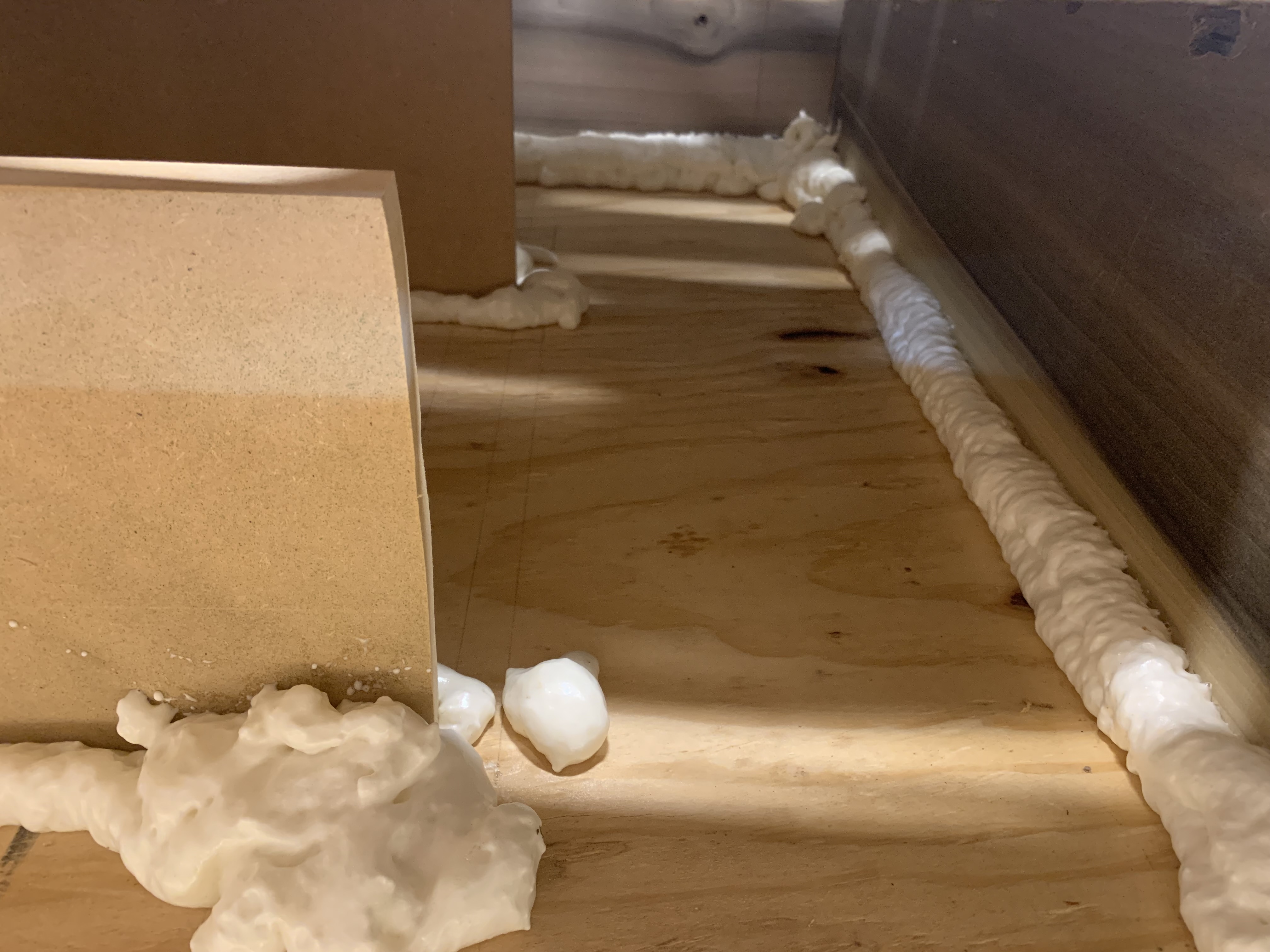
Figure 1: Foam
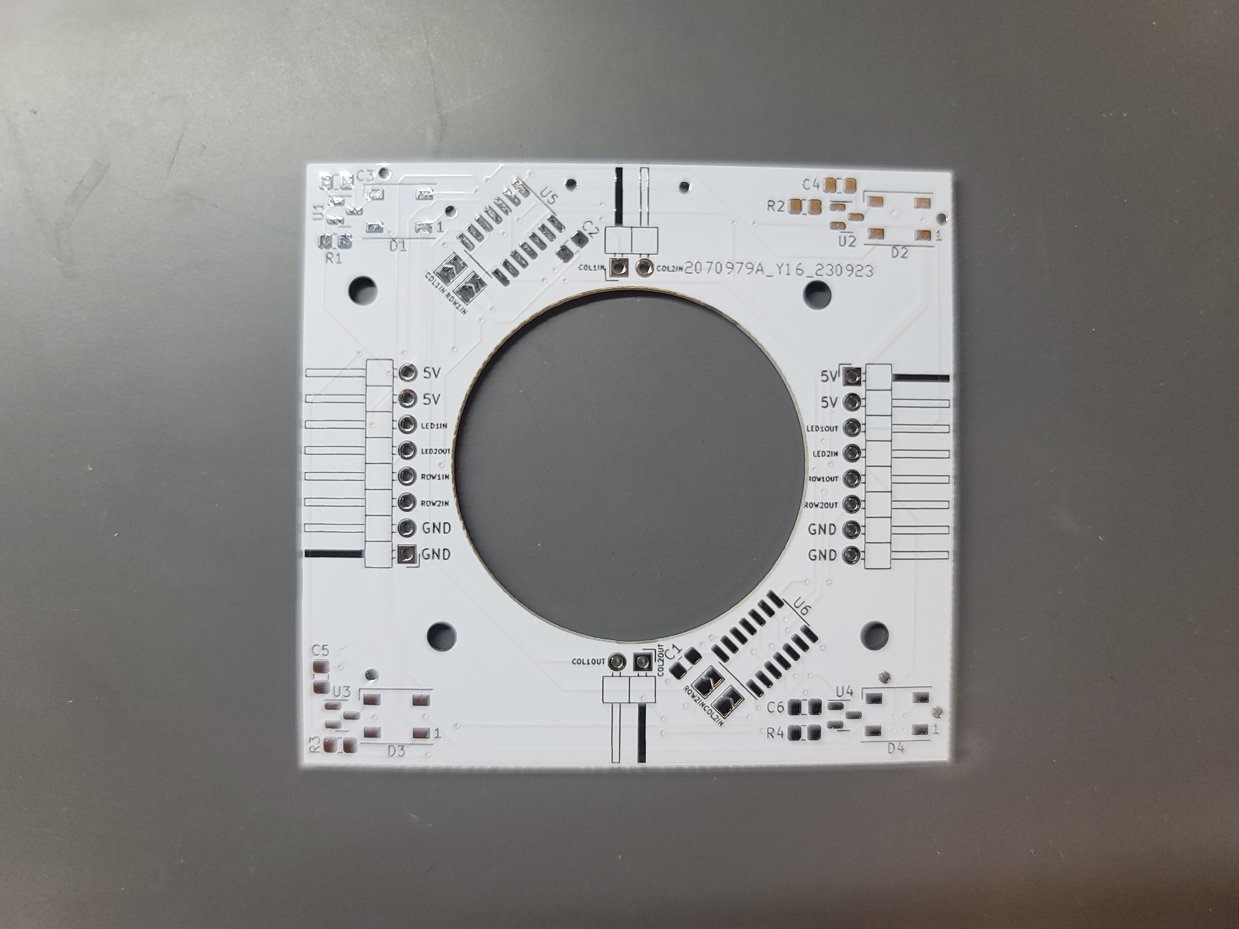
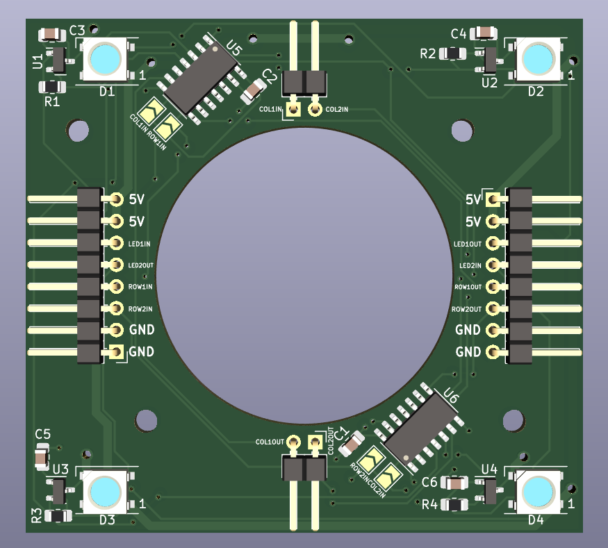
PCB soldering, mounting, and wiring
We soldered the remaining sets of pin headers to the PCBs. Afterwards, we mounted them to the MDF with small screws and began the tedious process of wiring the boards together. A picture of this process can be seen in Figure 2.
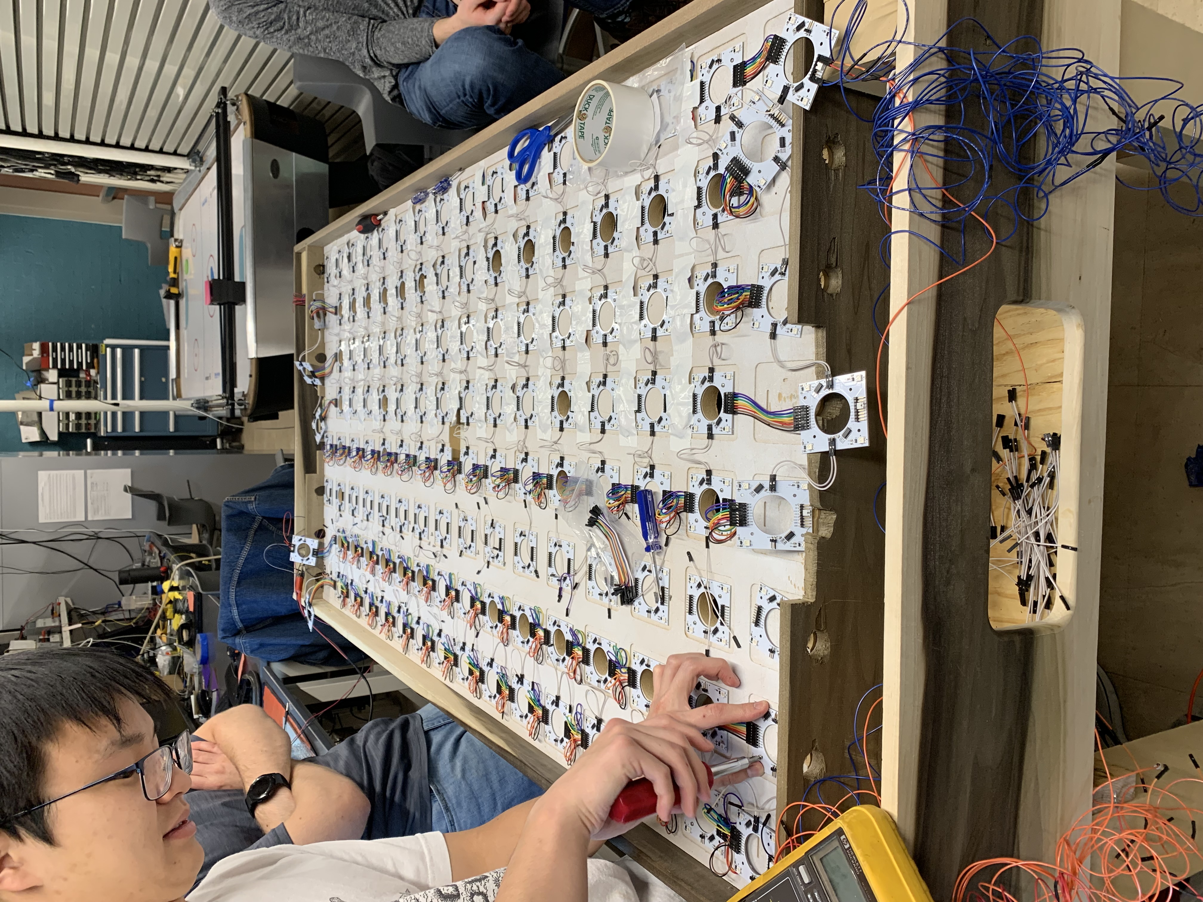
Figure 2: PCBs
Bus bars
Trevor and I cut and soldered the bus bars, providing 16 sets of power to the PCBs on the table. These are connected to our 5V power supply and dispurses the power to all PCB rows. This is necessary to avoid voltage drop and power loss (heat) for a maximum of around 100W of power when the LEDs are all on full brightness. A picture of one of the bus bars can be seen in Figure 3.
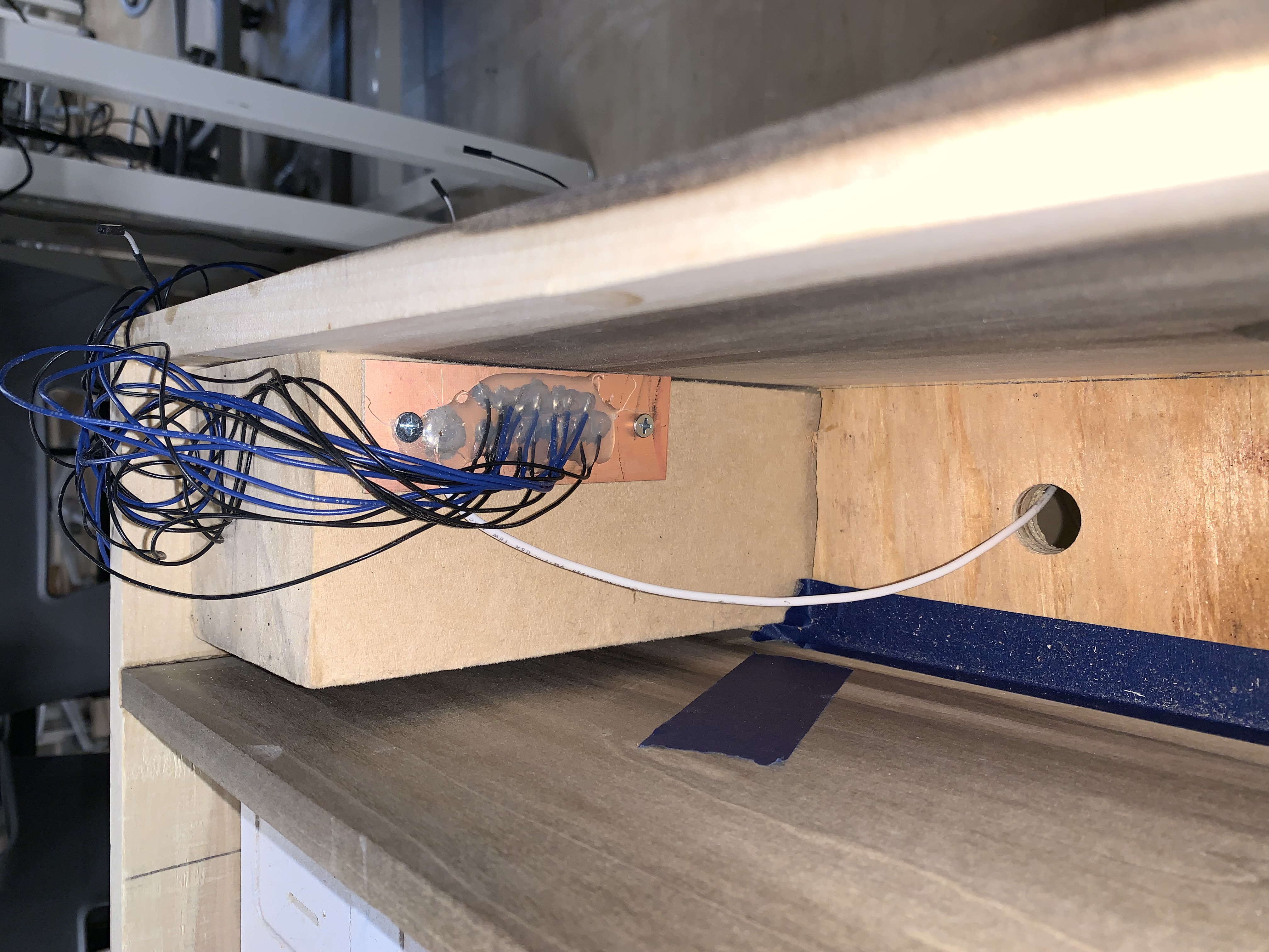
Figure 3: Bus bars
PCB external wiring
Once the PCBs were mounted and wired together, we had to wire the LED signal connections and hall effect sensor connections to the master PCB. Afterwards, we tested these connections before mounting acrylic.
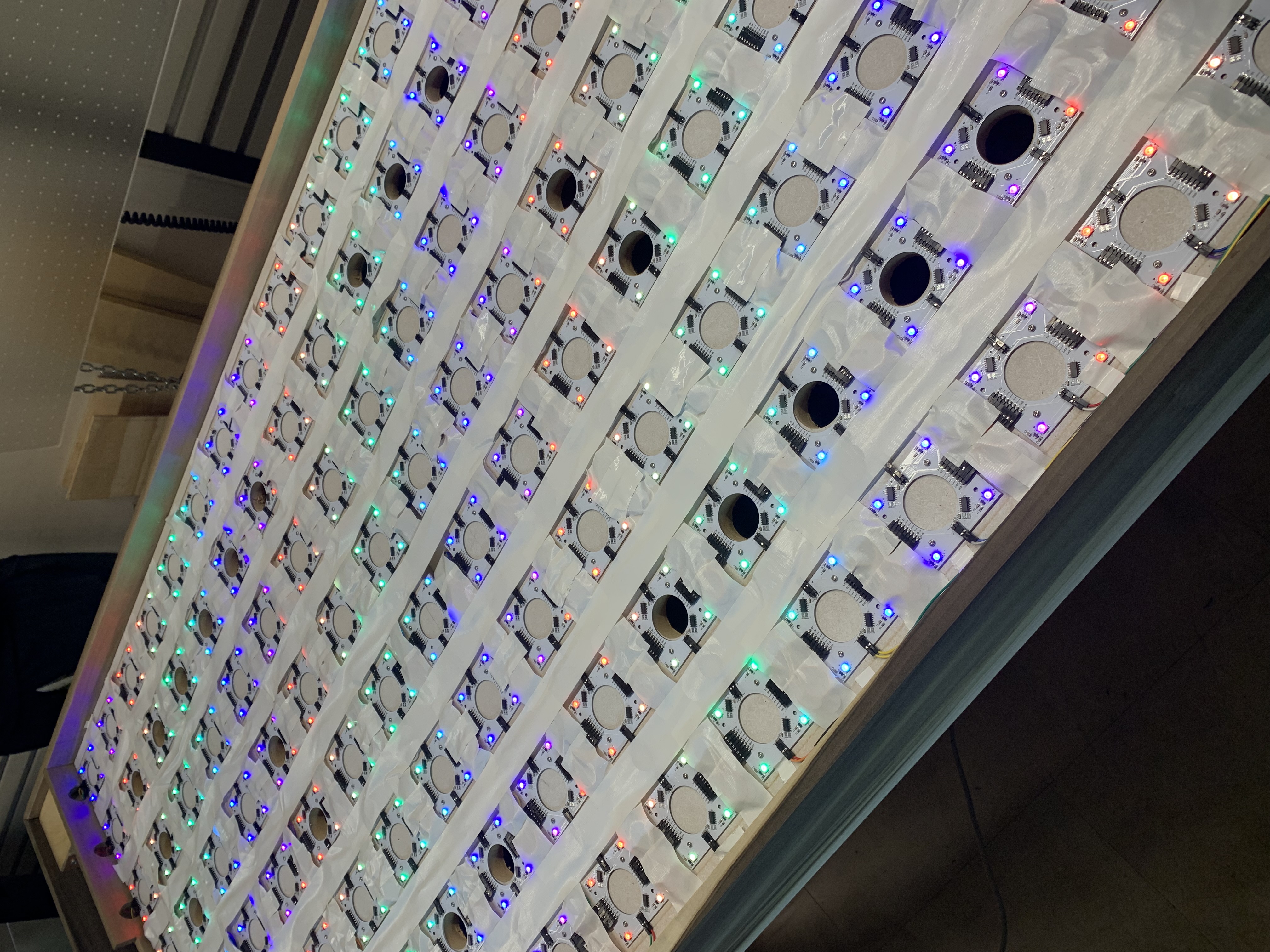
Figure 4: Testing sensor PCBs
Mounting acrylic
I designed and 3D printed the spacers to hold the acrylic sheet. This allowed us to mount the acrylic in its final position and test the hall effect sensitivity. A picture of this testing can be seen in Figure 5.
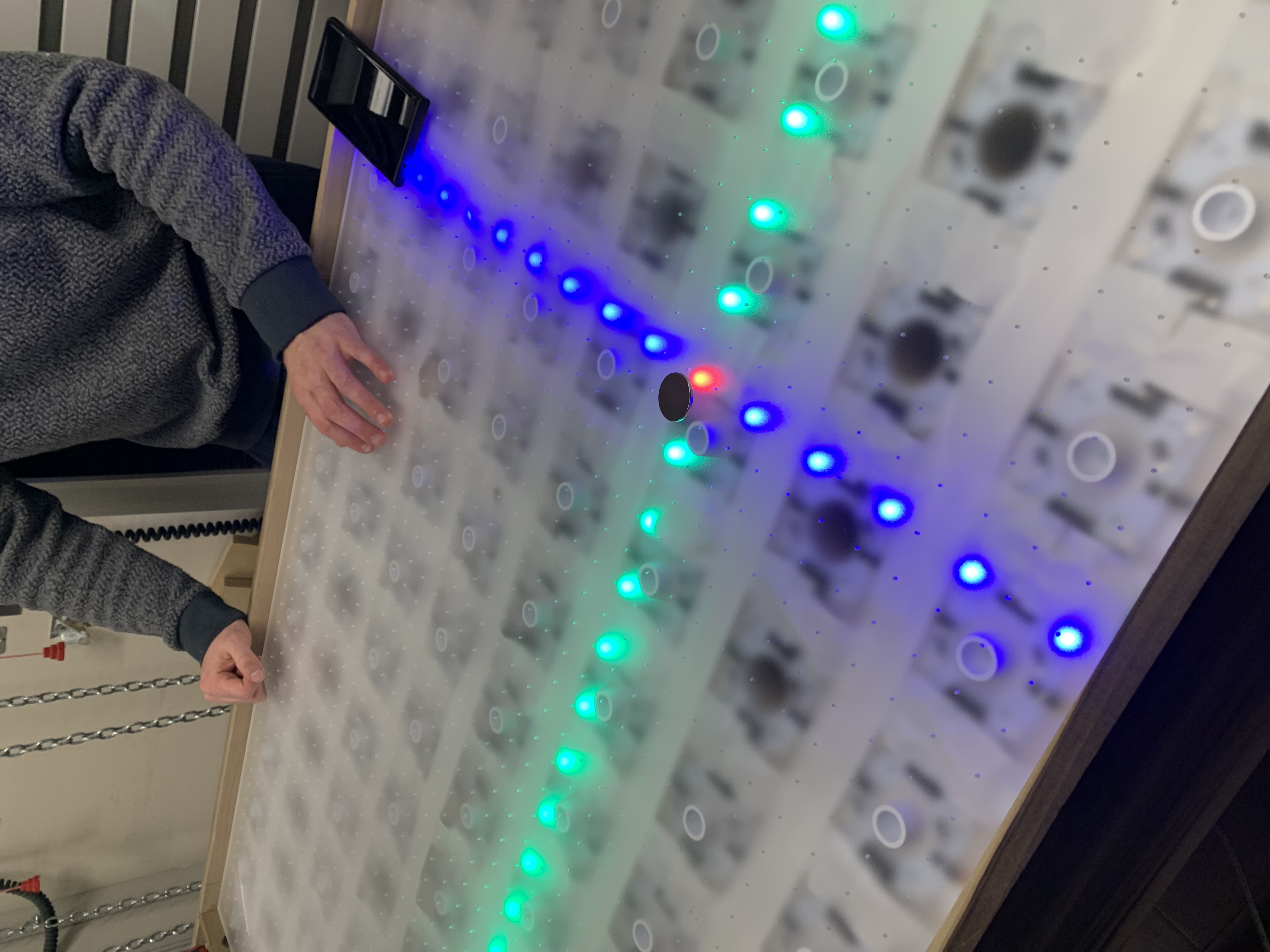
Figure 5: Hall effect testing
EEPROM testing
Trevor and I worked on the EEPROM to meet our bonus PSDR. For this, we probed onto the EEPROM with our Revision A master PCB and used the scope to look at the SPI signals. We figured out multiple issues and added a driver to read and write to the EEPROM, which is how we store/load game information and load some animation data for the PSDR.
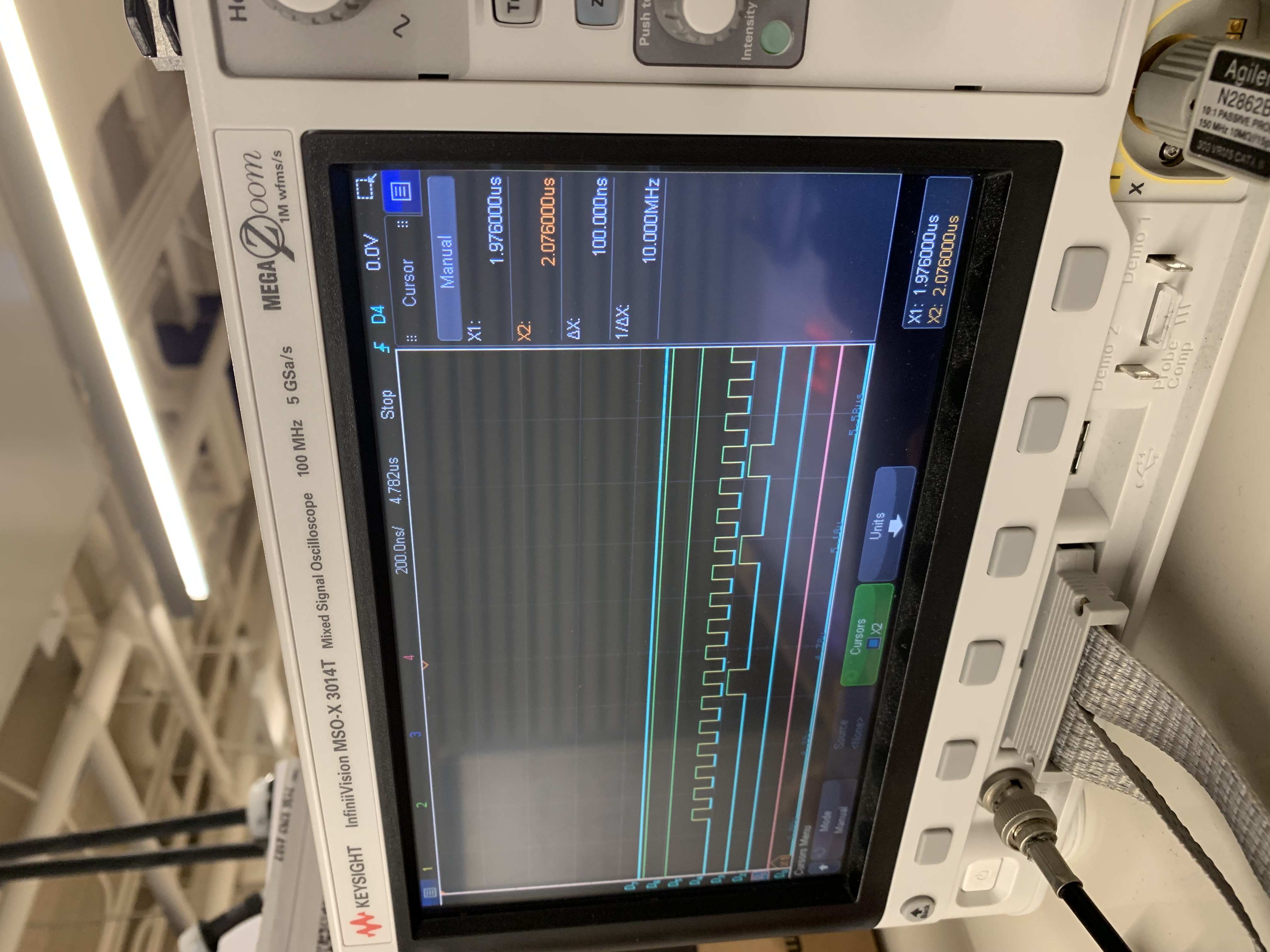
Figure 6: EEPROM probing
Goal detection and mounting
We printed and mounted the puck goals into their final position, gluing the LDR and LED pairs for goal detection. The following sections have no images due to the time during the day when they were completed :)
Top cover manufacturing
We assembled a top cover for the goal areas using thick cardboard from our acrylic shipping box and duct tape. This provides a smooth surface and a nice surface finish.
State machine
With final hardware, we finished the game logic state machine to handle a menu system, lighting effects, puck trail, goal detection, scoring and winning animations, and everything else involved in the game.
Project demo
We also had our project demo, and met all 5 PSDRs and both bonus PSDRs.
Next steps
- Finishing touches for SPARK challenge
Week 13
Date: 2023-11-17
Project Hours Since Last Report: 14
Total Hours: 162
Description of Project Design Efforts
Lots of progress mechanically.
Blower mounting
Trevor and I mounted the main blower fan and the outlet relay so we can control it with our master PCB. We marked the exact middle and cut out a hole for the blower using the jigsaw. We then screwed the blower in place and mounted the relay to power the fan.
A picture of the mounted blower can be seen in Figure 1.
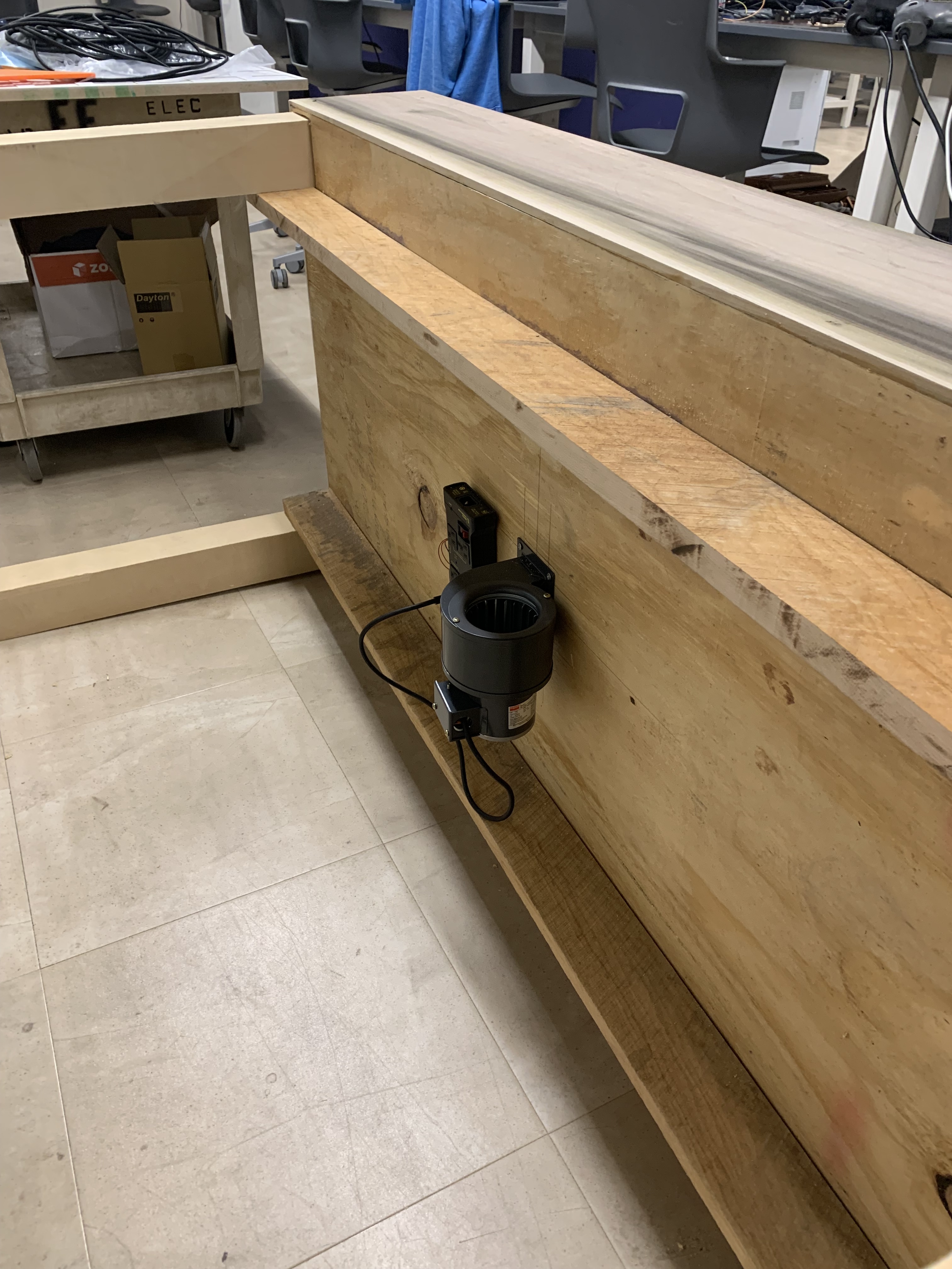
Figure 1: Blower
Table support beams
We noticed that the bottom plywood panel was delaminating in places due to the small glue contact area and the increased weight it was supporting. To remedy this, Trevor and I took some scrap boards from BIDC and cut them to length, which we mounted to the main table legs. This increases table rigidity and supports the plywood from the bottom. When we mount other items in the table, these will easily be able to support additional weight.
A picture of the support beams can be seen in Figure 2.
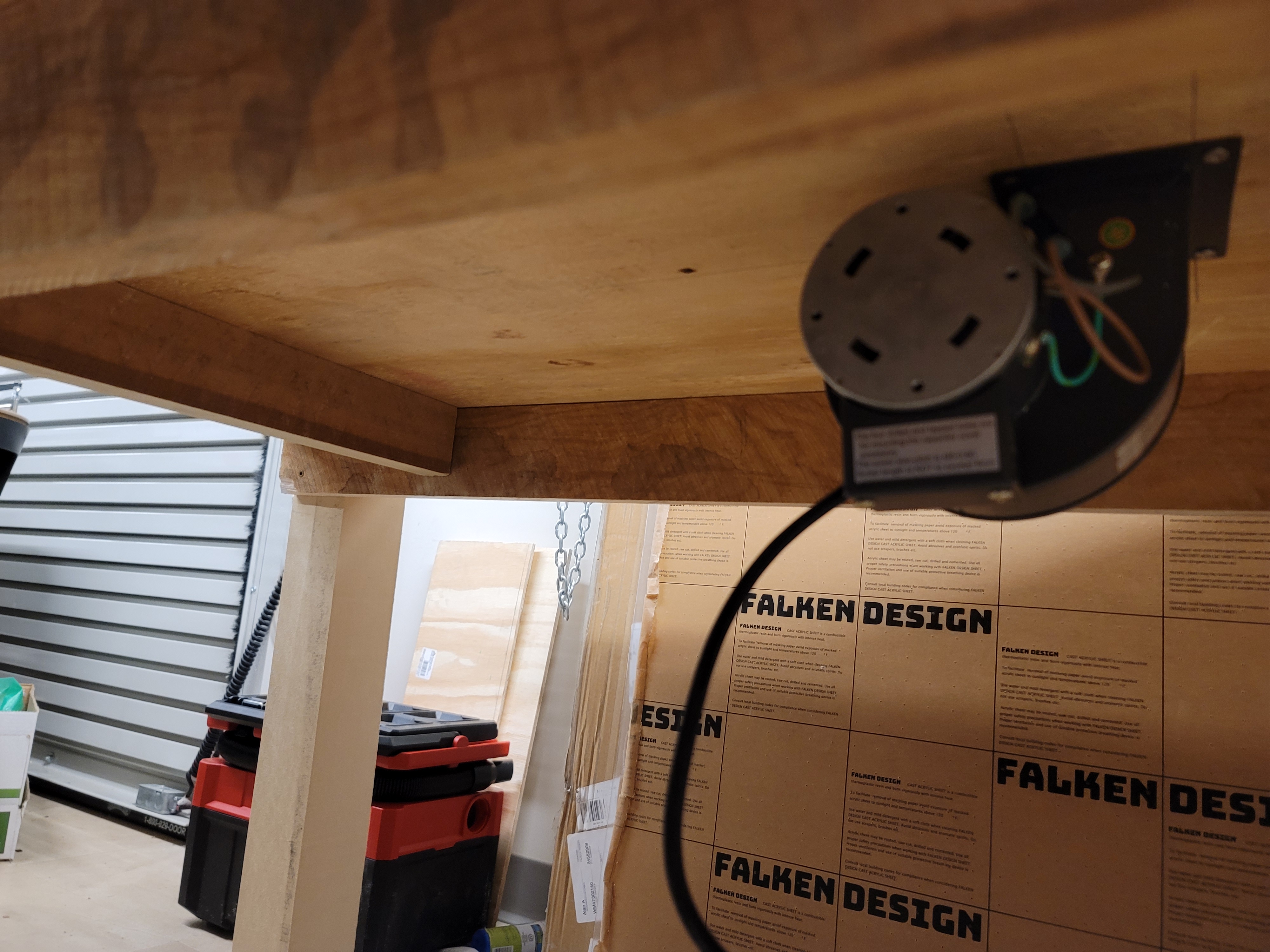
Figure 2: Support beams
Acrylic cutting
This was the largest chunk of time this week. Alan worked on designing the CAM model to cut our acrylic sheet on the gantry, and I went and helped him for the manufacturing. This invovled any changes to the file, preparing the gantry surface, supervising the machine in the event of any malfunctions, and cleanup and transportation of the acrylic after completing. This took many hours, but the acrylic came out very clean. We left the protective sticker on the acrylic to avoid scratches.
A video of the gantry in action can be seen in Figure 3.
Figure 3: Gantry cutting acrylic
Test fitting for final mechanical assembly
The last thing we did this week was testing all of the mechanical pieces together. We put supports on the bottom plywood to support the MDF, cut a hole in the MDF for airflow, and added spacers and the acrylic sheet on top. After turning the air on, we were greeted with so much air pressure that the acrylic sheet was bulging. This ended up being so much air that it wasn’t coming out of the holes very quickly. We have two solutions which should help greatly. First, we are going to cut more holes in the MDF to allow more even airflow. This will help with the bulging. Second, we will likely drill larger air holes in the acrylic. This should promote airflow (since our blower is so powerful), and will allow more air to escape, also helping with the bulging issue.
A picture of everything in place (testing) can be seen in Figure 4.
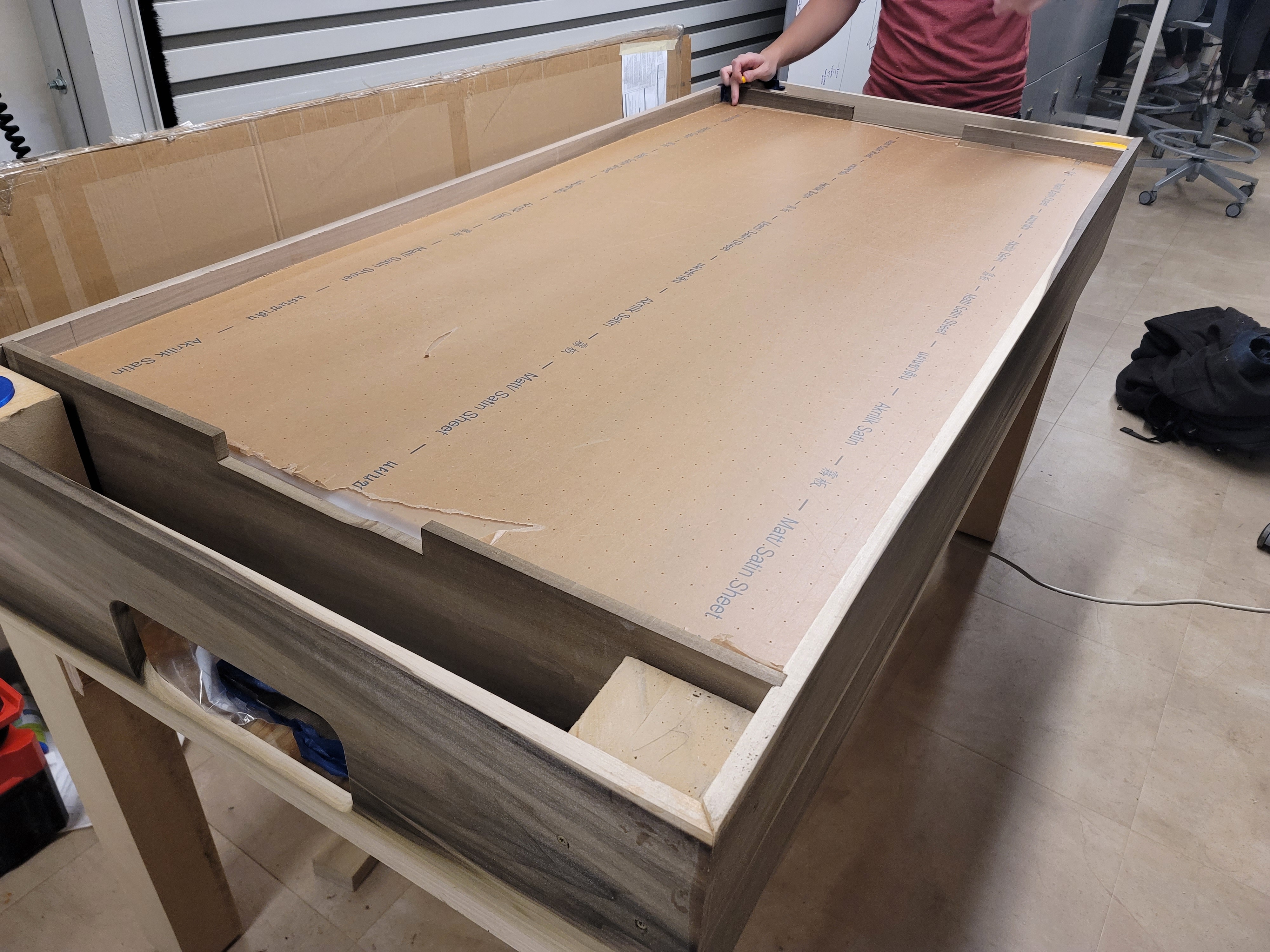
Figure 4: Final testing before mounting
Next steps
- Blower testing for final airflow and assembly
- Bus bar/PCB mounting/wiring
- Mount power supplies
- Assemble puck goals and connect external components
- Mount master PCB
Week 12
Date: 2023-11-10
Project Hours Since Last Report: 16
Total Hours: 148
Description of Project Design Efforts
With Alan out of town for a conference, we focused most of our time on mechanical progress.
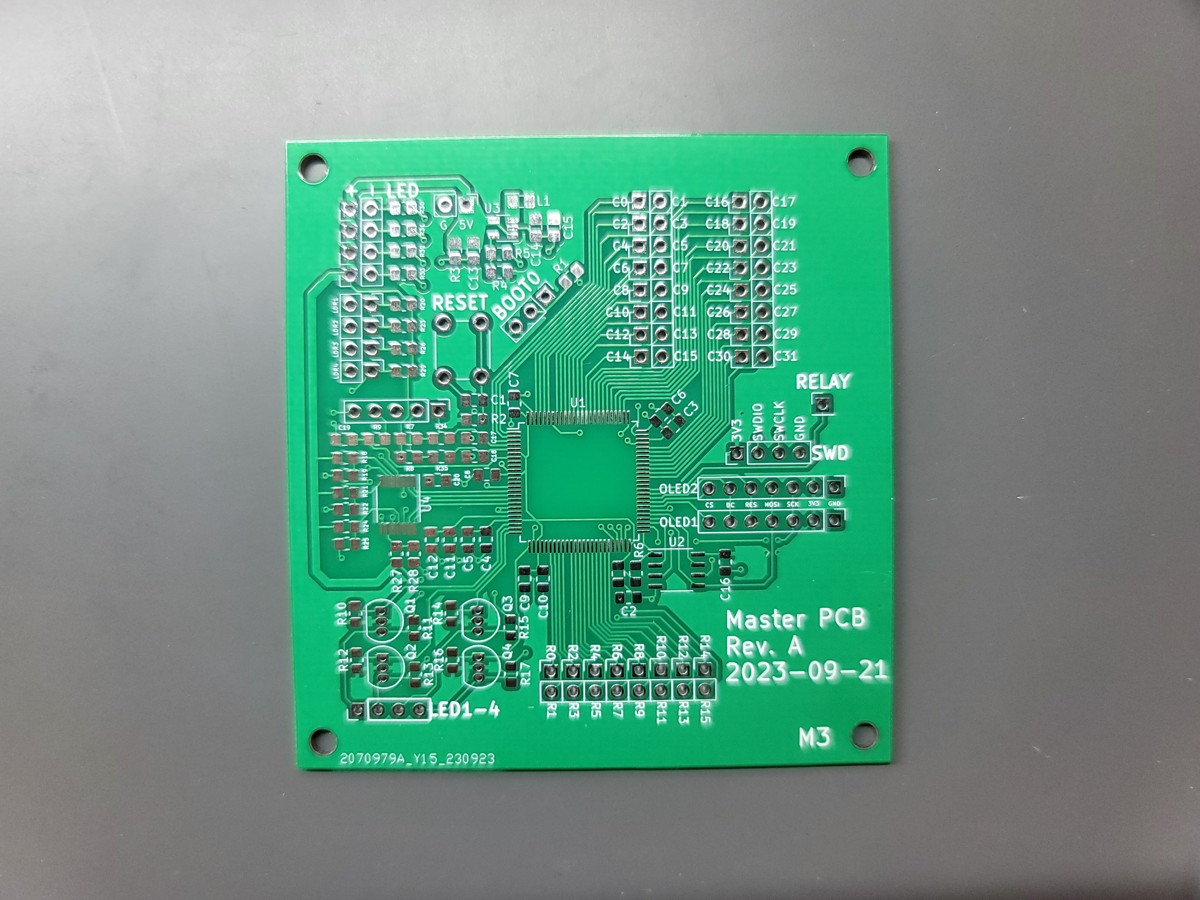
Master PCB assembly/testing
I finished soldering the master PCB and testing each of the components. We were able to get all of our PSDRs checked off (preliminary) and verified that everything on our board works as expected.
A picture of the master PCB can be seen in Figure 1.
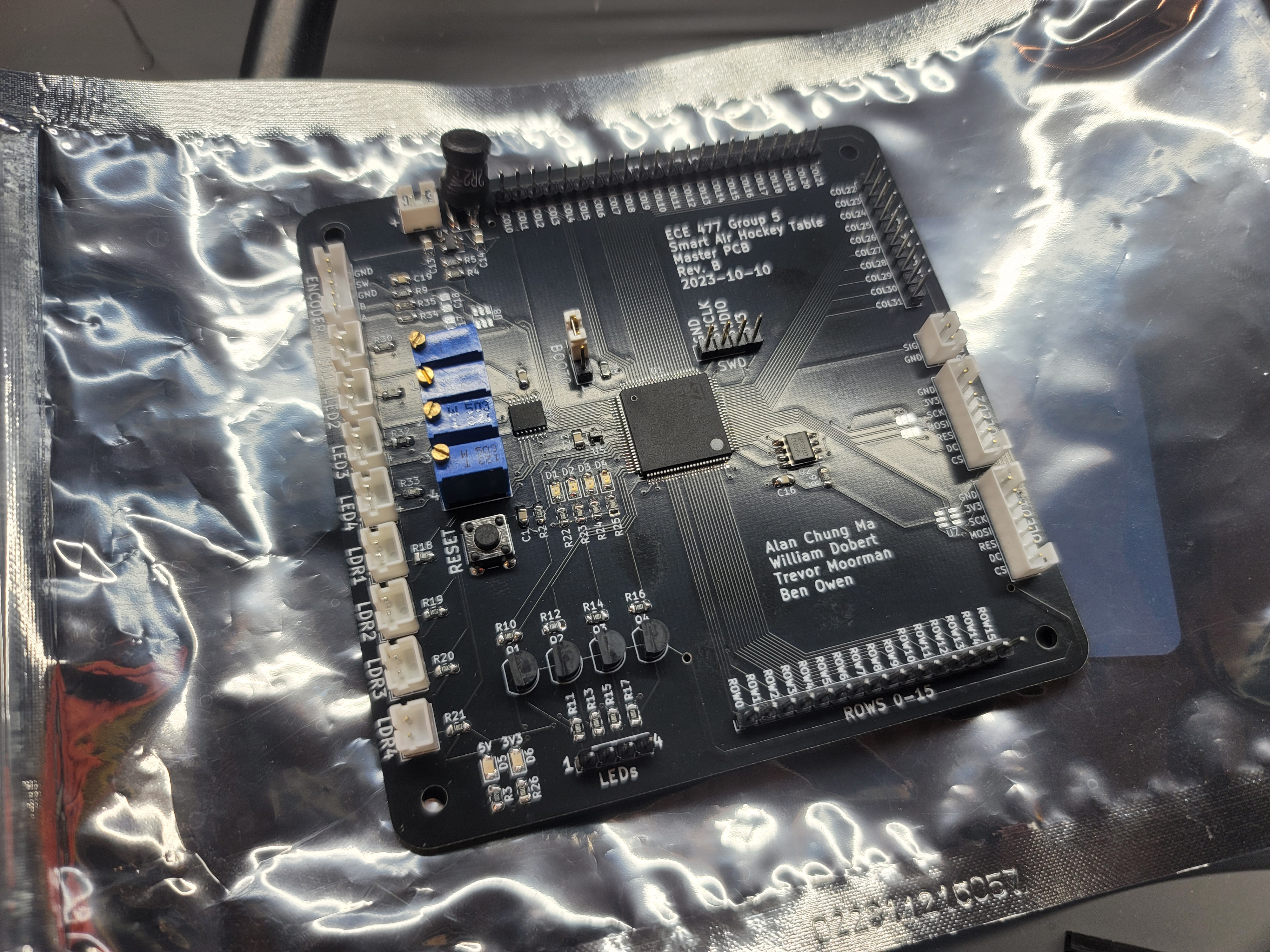
Figure 1: Master PCB
One of the other things we tested was our motor encoder, which is demonstrated in Figure 2.
Figure 2: Encoder demo
External connections
For the master PCB, there are a number of components that are far away from the PCB. These include the OLED displays, menu encoder, and LDR/LED pairs. I spent a lot of time crimping connectors for these components and putting them inside of wire looms for durability. Currently, I have completed all 4 LEDs, all 4 LDRs, 1 OLED display, and the motor encoder. The remaining connectors are the other OLED display and the relay connector for turning our blower motor on/off.
A picture of these can be seen in Figure 3.
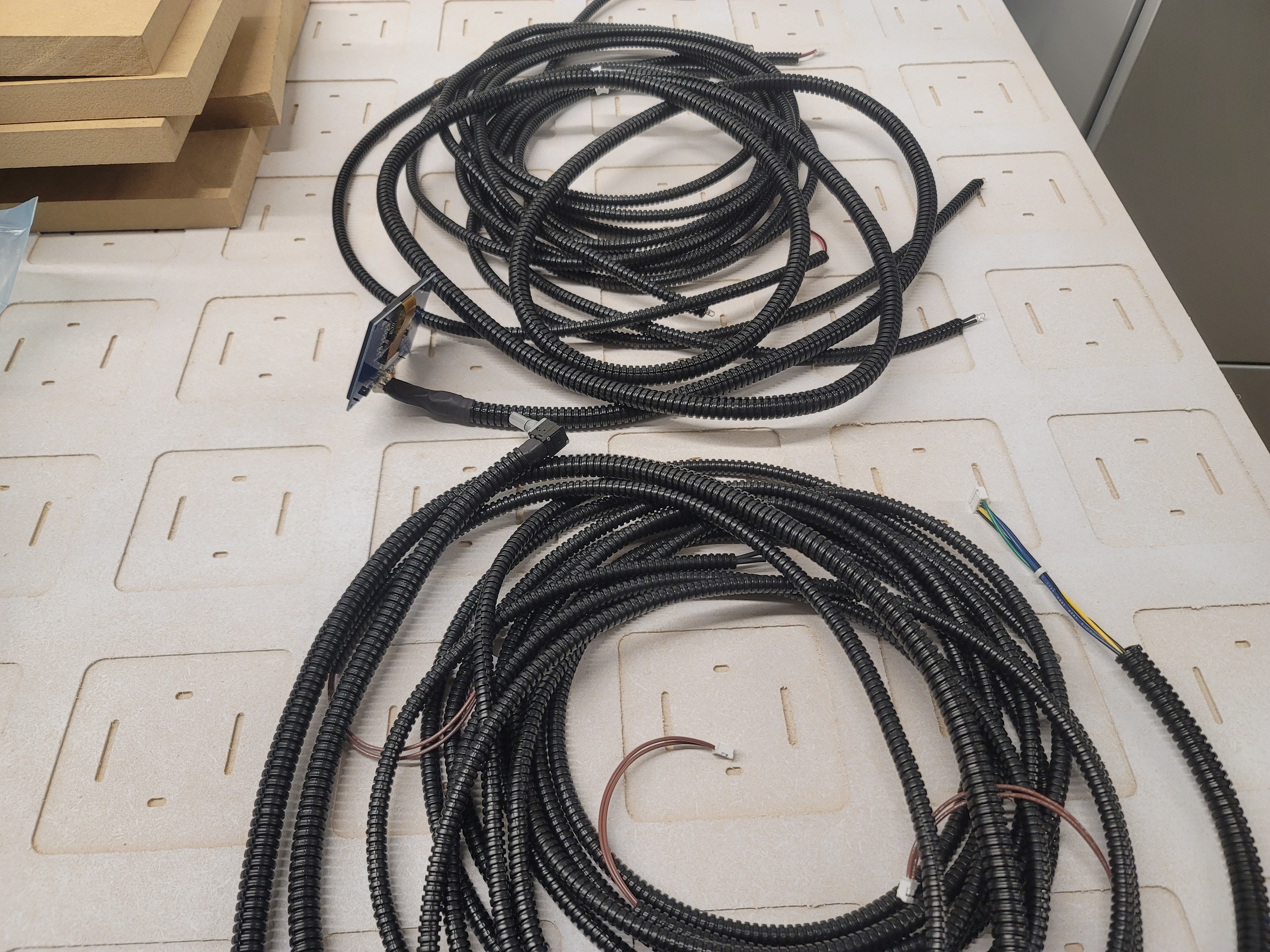
Figure 3: External components
Mechanical progress
Since Alan was out of town, we focused on making progress on the mechanical aspects of the table. Mainly, we need to begin mounting the blower and other electrical components, since we have verified our PCBs functionality. Therefore, we spent a number of hours finding wood for table legs and getting it cut to the correct size at BIDC. We then cut out holes in the bottom plywood to inset the legs up unto the table for strength. Four screws hold in each of the legs to the table. Then, we added support beams along the long edge of the table connected to the table legs. This ensures that
An image of the current table can be seen in Figure 4.
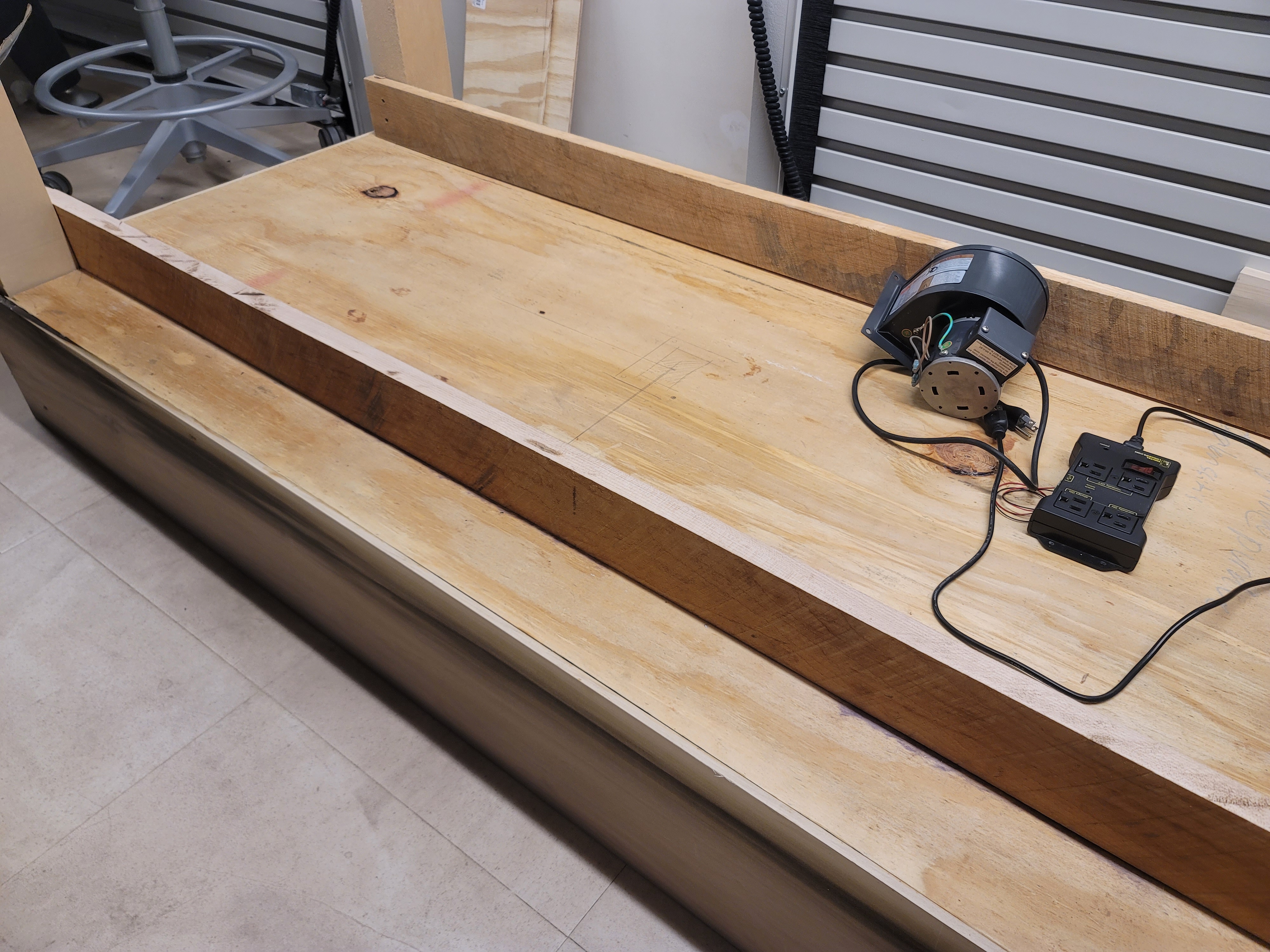
Figure 4: Table (upside down)
Next steps
- Mechanical progress
- Mount blower to plywood
- Mount outlet to plywood
- Mount 5V PSU to plywood
- Add internal MDF supports for sensor PCB mounting board
- Electrical/mechanical progress
- Create “bus bar” for our sensor PCBs out of unmilled copper board
Week 11
Date: 2023-11-03
Project Hours Since Last Report: 10
Total Hours: 132
Description of Project Design Efforts
This week was exam week, so major progress wasn’t made.
Acrylic Spacers CAD
I worked on designing some spacers to go between the MDF and top acrylic layers. This was designed in FreeCAD, and allows for easy manipulation of parameters such as height, screw diameter, overall diameter, etc. I will be 3D printing some of these this upcoming week to test them out and see if we want to make any changes to them, but the plan is to use these to support the acrylic.
A picture of the CAD render can be seen in Figure 1.
Figure 1: Acrylic spacers CAD model
Sensor PCB Testing
Trevor and I spent a lot of time unpacking the assembled sensor PCBs and getting them prepared for testing. They arrived with V-scores along the edges, so we snapped all 4 edges off for each of the assembled boards. After laying them out on the MDF, we were then able to solder the position jumpers (for the first row/column PCBs) and pin headers. This allowed us to finally test our design over a full 16-PCB length. Luckily, our circuit works as expected, and we were able to propagate hall effect data and LED data along the entire string of PCBs. However, we don’t want to do stress tests at this time, as our power delivery is starting to become less safe (pulling 2 amps continuous through a small breadboard jumper is not the best idea).
A picture of the delivered sensor PCBs (unassembled and assembled) and our MDF with the PCBs on top can be seen in Figures 2 and 3.
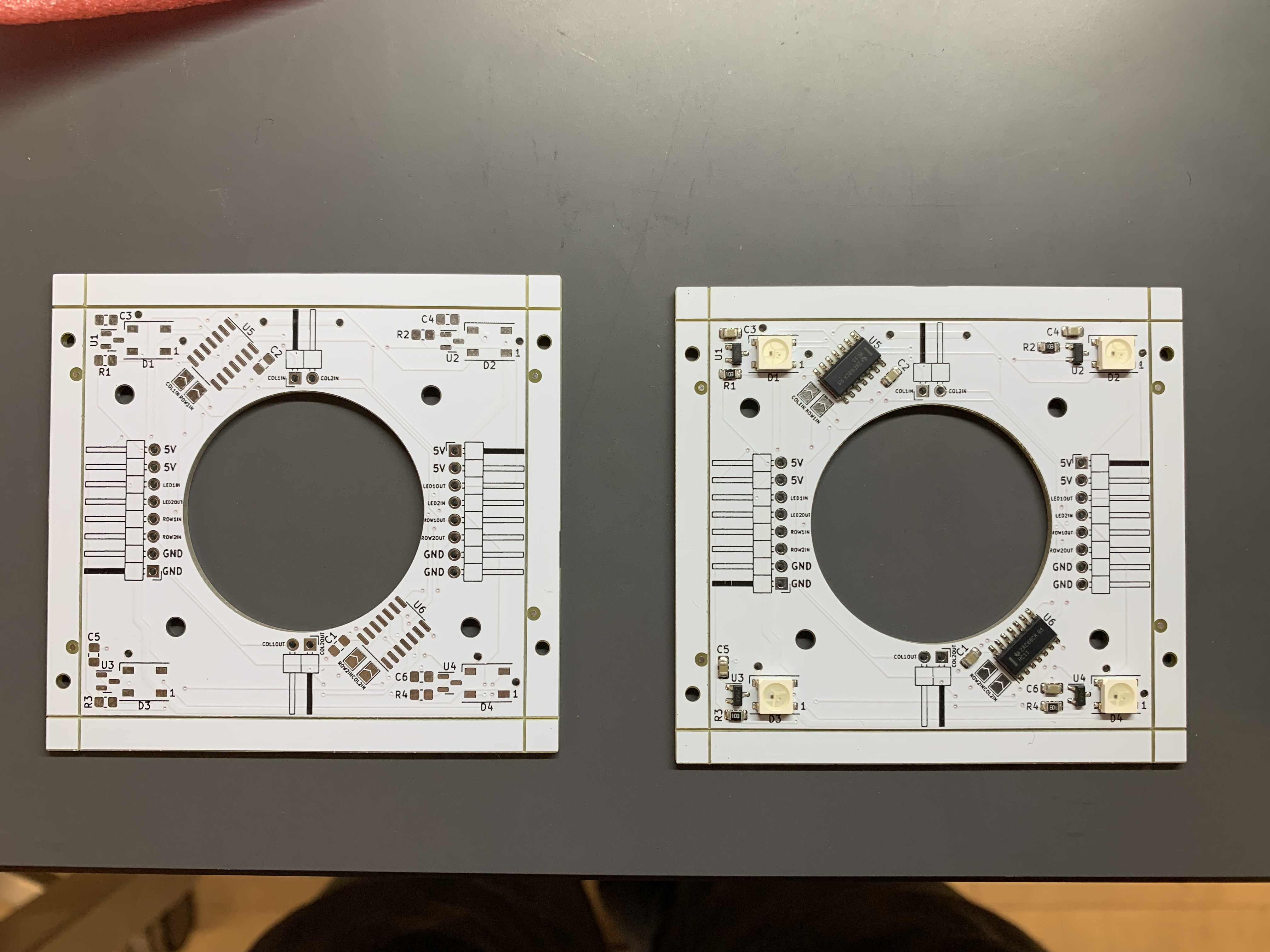
Figure 2: Sensor PCBs
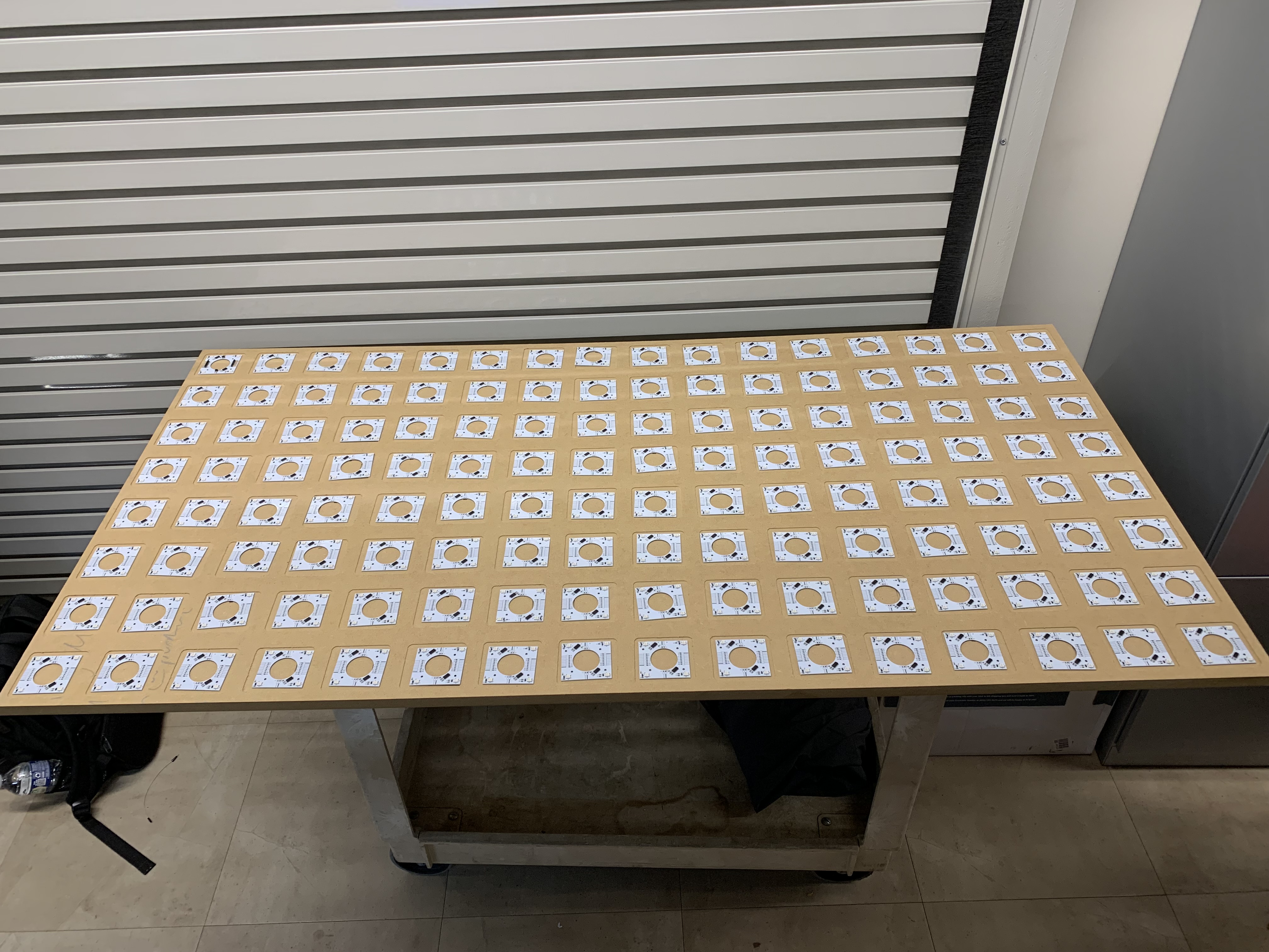
Figure 3: PCBs on MDF
Master PCB assembly
The Digi-Key items arrived later than expected, so we weren’t able to fully solder our master PCB this week. However, we were able to test our microcontroller connection and our buck converter, which are the two most critical components of our board.
To start, Digi-Key didn’t ship our inductors with the rest of our order, so we had to improvise to test this buck converter. To do this, Trevor and I went to the EE shop and found a through-hole inductor with a suitable current rating. We then bent the THT leads to allow the inductor to sit flat on the PCB, with the pins sitting on top of the SMD pads. We were then able to solder the component to the board and verify correct operation of our circuit.
Since the inductor should be rated for the low power we will be using, we plan to not replace this inductor when the parts eventually arrive. However, for our second master PCB (for backup use or other testing), we will wait to assemble that buck converter circuit until the correct inductors arrive. If we have issues with the buck converter circuit, we may switch the first PCB inductor.
An image of the jank inductor setup can be seen in Figure 4.
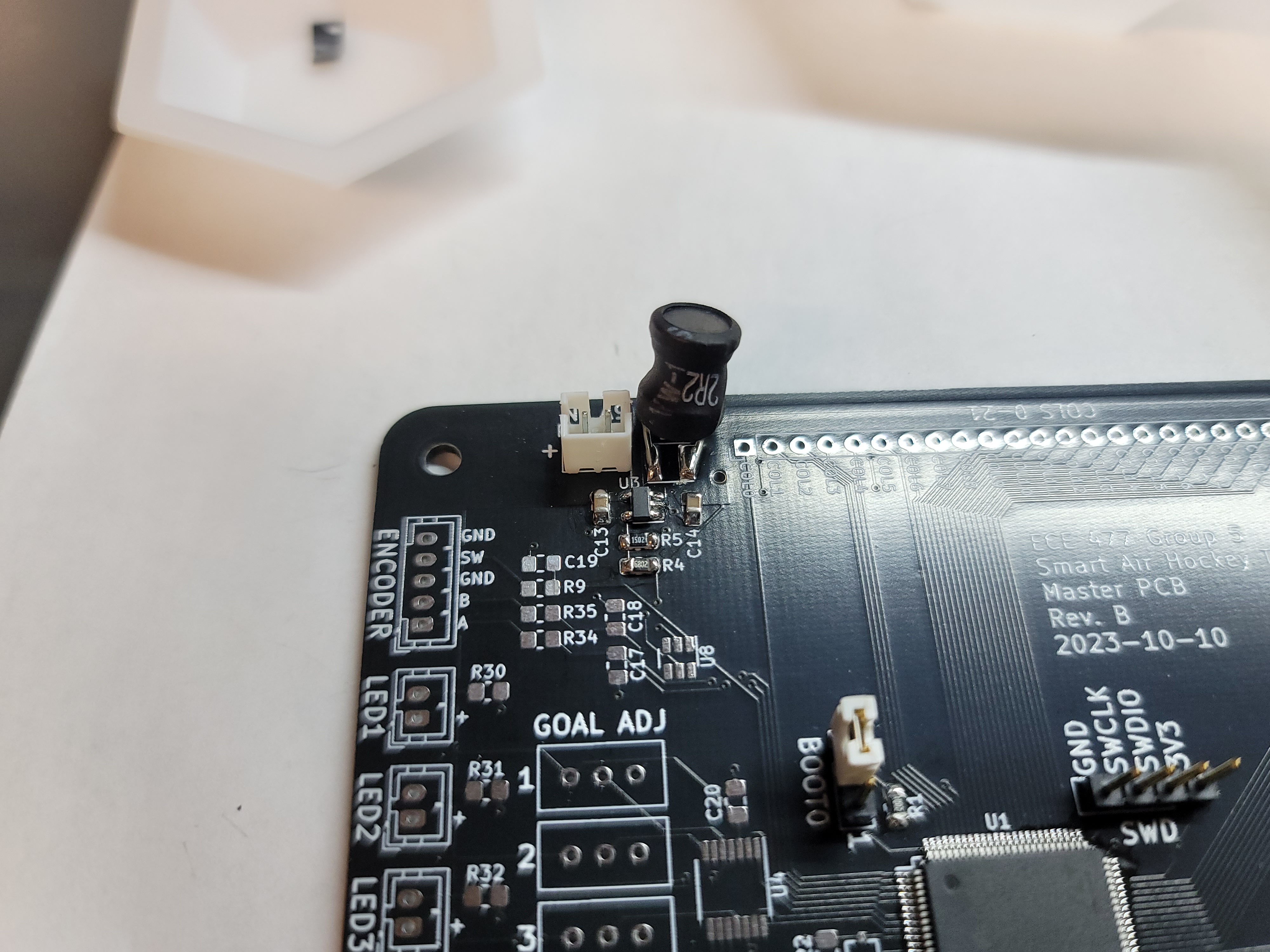
Figure 4: Wack inductor
After this was assembled, we had time to test our STM32 connection to our computer while being externally powered. To do this, I soldered the STM32 along with the minimum supporting components (BOOT0 jumper, reset passives, and programming header), and after verifying no shorts across power planes, connected the programming header to my computer while powering the STM32 through the buck converter. We were able to successfully connect to the microcontroller, which tells us that our STM32 is working normally at this point. This was also enough to check off one of our PSDRs relating to the buck converter powering the STM32.
An image of the minimum-assembled PCB can be seen in Figure 5.
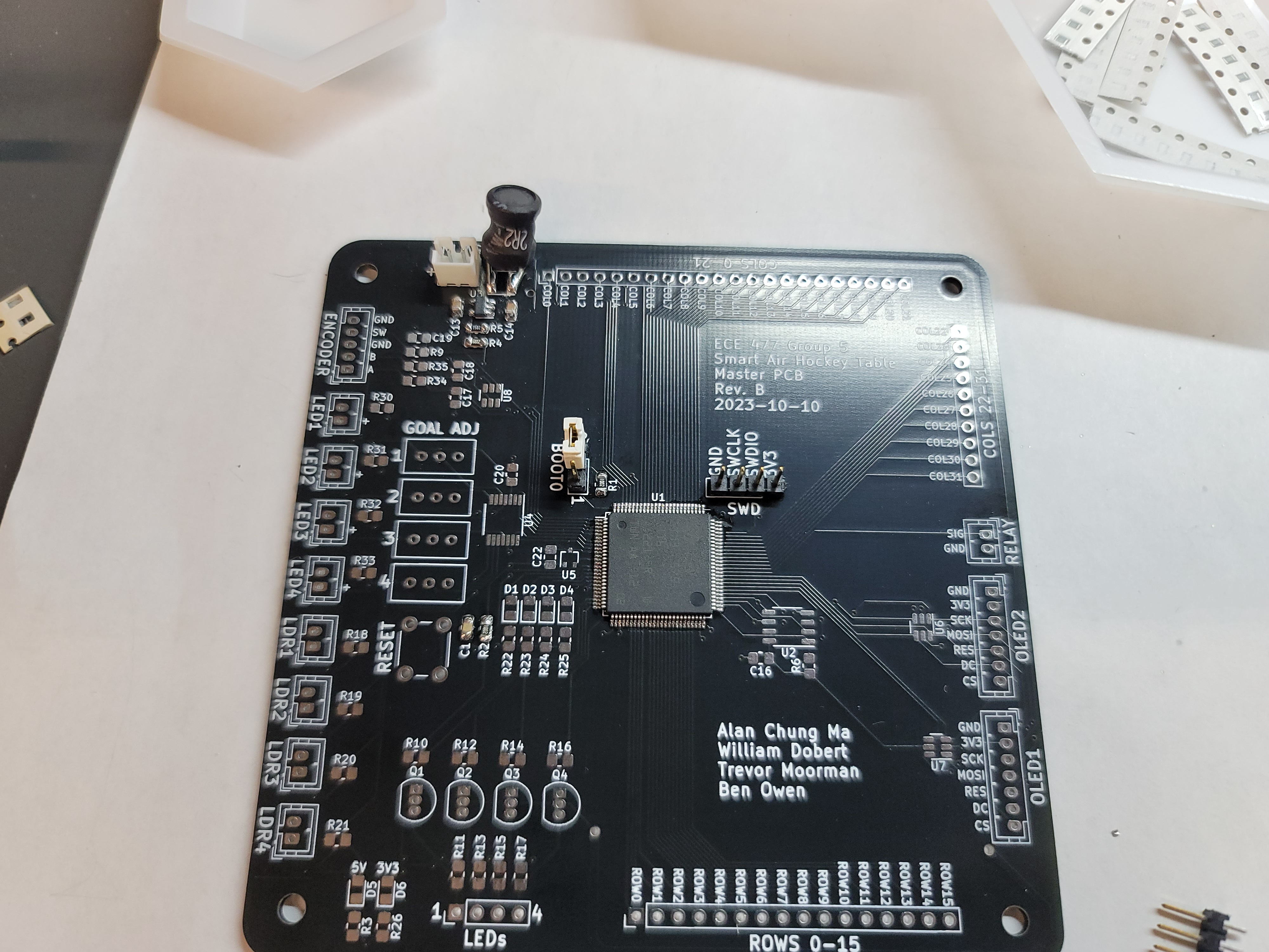
Figure 5: Partially-assembled master PCB
Next steps
EEPROM driver
Trevor and I both had multiple exams this week, so no times really lined up to work on this. However, our schedules are a lot emptier this upcoming week, so we plan on finishing it next week.
PCB assembly
We will finish assembling our master PCB and hopefully check off our remaining PSDRs (preliminary).
Week 10
Date: 2023-10-27
Project Hours Since Last Report: 8
Total Hours: 122
Description of Project Design Efforts
Table Construction
Alan worked a lot on the gantry files for the MDF mounting plate for our sensor PCBs, but he needed some help transporting the board and physically running the equipment. I went with Alan and Trevor to BIDC this week and spent a few hours getting the board cut successfully. We then relocated the table to our lab in EE. An image of this MDF with some PCBs on it can be seen in Figure 1.
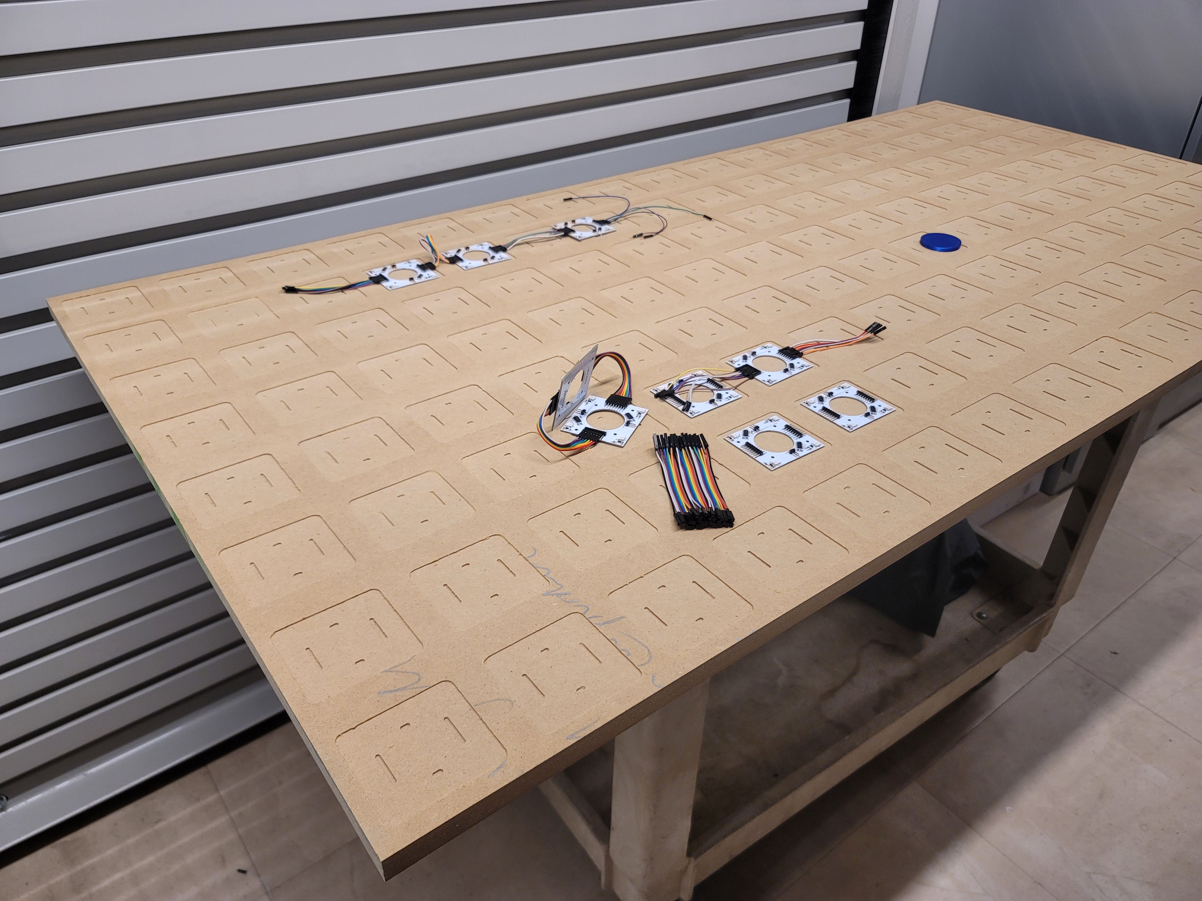
Figure 1: Sensor PCB testing
EEPROM driver considerations
Trevor and I are working on the EEPROM driver which is present on our master PCB. We spent a lot of time making calculations and discussing which instructions we need for our driver. Our current list of instructions are shown in Figure 2.
// Necessary instructions
WREN: write enable
WRDI: write disable
RDSR: read status register
WDSR: write status register
FREAD: fast single data read
PGWR: page write (erage and program)
CHER: chip erase
RSTEN: enable reset
RESET: software reset

// Stretch instructions
DPD: deep power-down enter
RDPD: deep power-down release
Figure 2: EEPROM instructions
A big calculation we performed was best-case time to load an entire table frame. To calculate this, we take the amount of data for an entire table (512 LEDs _ 3 bytes per LED _ 8 bits per byte) and add it with the instruction to send to EEPROM (8 bits per instruction + 24 bits per address + 8 “dummy” bits for faster reads). This is a total amount of data of 12,328 bits, or 12,328 SPI clock cycles. At 80 MHz clock (the fastest the EEPROM supports for these instructions), this takes around 150 uS. Since our game tick is currently set to 1 ms, we are optimistic that we would be able to read an entire animation frame in a single game loop. If proven, this would allow us not need to coordinate partial animation frame loads. We hopefully will be able to test this next week.
Next steps
Sensor PCB testing
When our assembled sensor PCBs arrive, we need to test each of them for correct operation. We will then line them up on our now finished MDF backing plate and connect them together. This will allow us to do large-scale testing in the coming weeks on final hardware.
EEPROM driver
For bonus PSDRs and ease of use, we need a driver to interact with our EEPROM. To do this, we will implement the instructions mentioned in this week’s progress report (as well as some others such as write protection).
PCB assembly
PCBs should be arriving this week with components, so I will be assembling and testing the master PCB.
Weeks 8-9
Date: 2023-10-20
Project Hours Since Last Report: 20
Total Hours: 114
Description of Project Design Efforts
Midterm Design Presentation
We spend a lot of time putting together and practicing our midterm design presentation. We were the first group presenting. A link to our final presentation can be seen on the Documents page of our website.
Sensor PCB Soldering/Testing
We wanted to be able to test a longer strip of PCBs in order to confirm our hall effect and individually-addressable LED configuration for the final run of boards. I spent a lot of time soldering new sensor boards, and fixing some that weren’t soldered correctly. We were able to confirm that our hall effect AND gate logic works perfectly, and scales well across longer and longer PCB runs. We also confirmed that there were no apparent issues with the LEDs, as signal could be transmitted along and back the entire 9-board configuration.
A picture of this long sensor PCB testing can be seen in Figure 1.
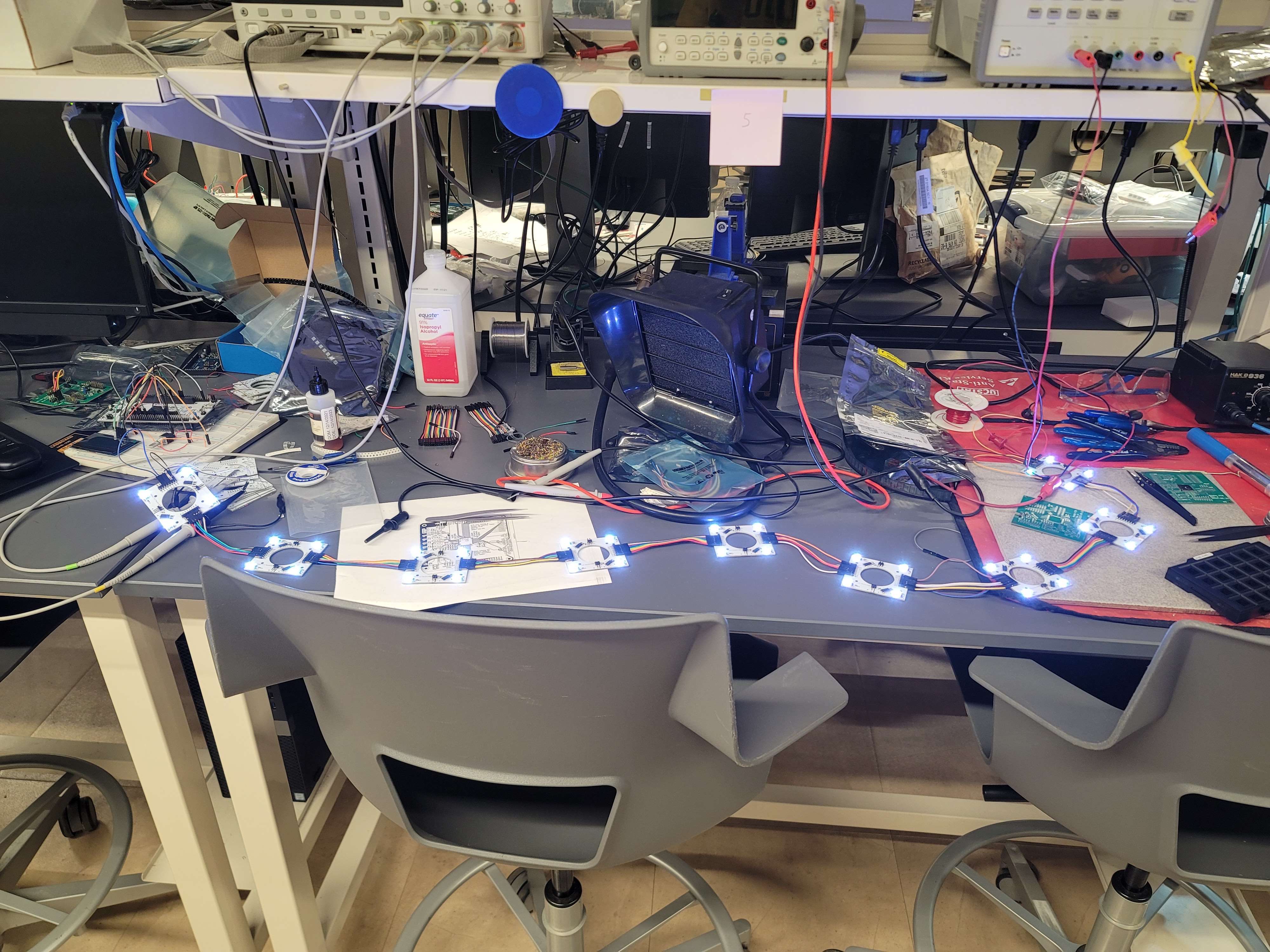
Figure 1: Sensor PCB testing
Master PCB external power test
We finally got a chance to test our onboard buck converter on the master PCB while powering the STM32. We prepared a simple program to flash to our STM32, and while powering with an external 5V source, we were able to program and read flash data from the microcontroller. A screenshot from this testing can be seen in Figure 2.
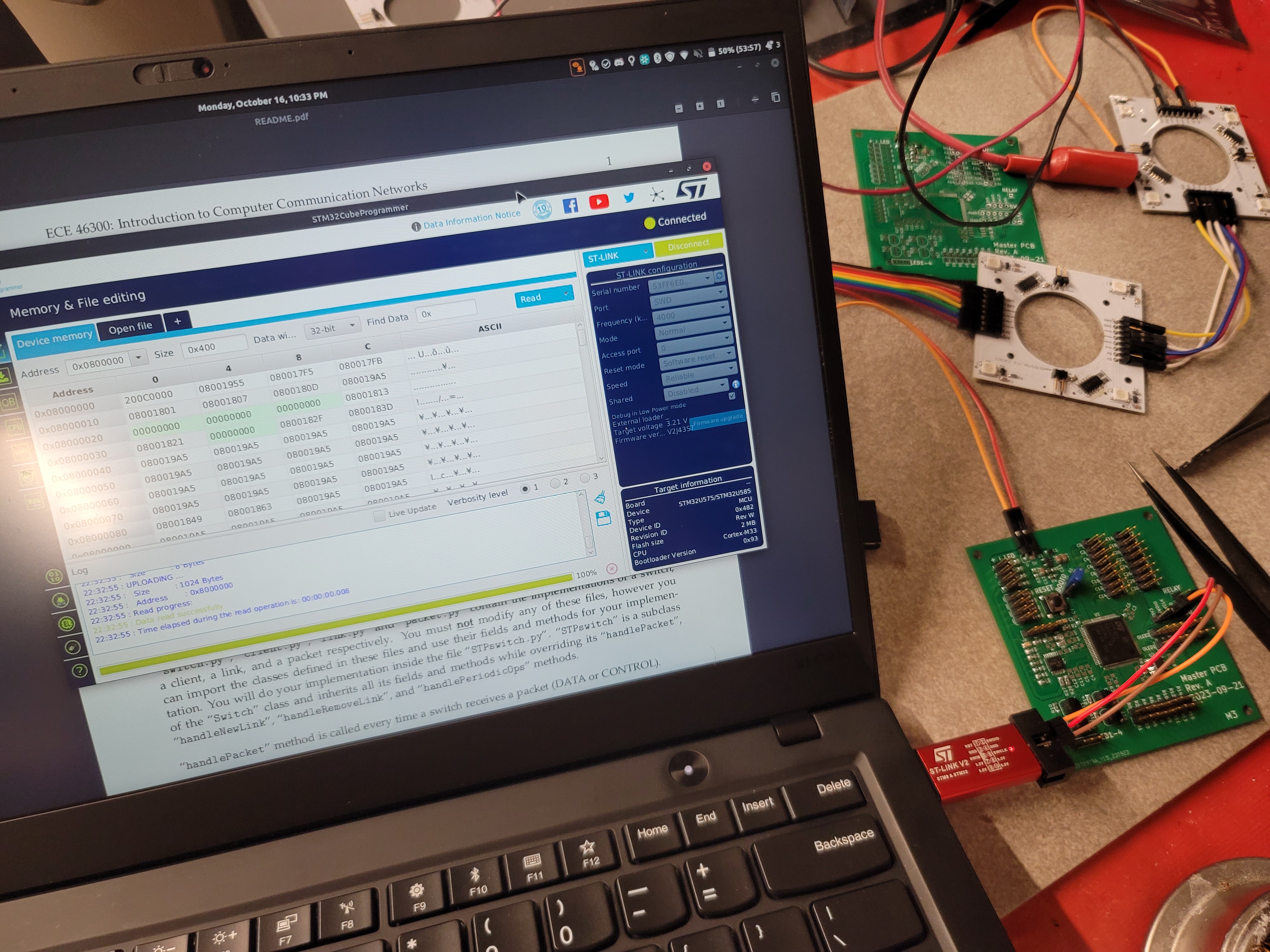
Figure 2: STM32 externally powered and connected
PCB reviews and ordering
For our master PCB, we already had Revision B finished and ready to order. However, upon preparing to order the second round of sensor PCBs, we decided to price out other suppliers for our components. After much discussion, we learned that JLCPCB’s assembly service was actually cheaper than us hand-soldering these boards, and it was more likely that the soldering quality would be higher. We then spend a long time preparing production files for JLCPCB assembly, sourcing part numbers and ensuring the pick and place files were correct.
A render from JLCPCB’s pick and place confirmation tool can be seen in Figure 3
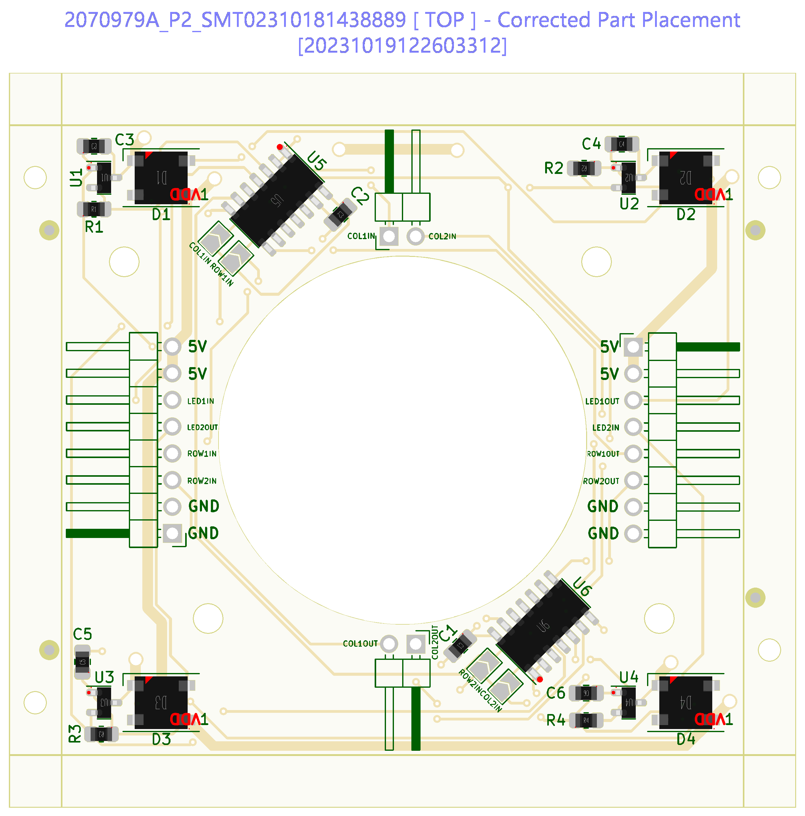
Figure 3: JLCPCB sensor PCB pick and place render
Drivers and state machine firmware
Since the PCBs are finished, I had a chance to work on firmware and prepare for implementing the entire sensor PCB array in a few weeks. This week, I helped write a driver to turn our outlet relay on/off. I also worked on a driver to read in our hall effect sensor row/column data and insert it into an easy-to-use variable. This involved a lot of planning and preparation to correctly shift each input data bit to the correct location. Code snippets for this driver can be seen in Figure 4. Full driver code and implementation are on our Github repository.
void Driver_HallEffect_PollInputs()
{
	// need to shift hall data to correct bit position
	// shift amount calculated by function (IDR bit position - desired bit position)
	//
	// example: ROW1 is on PA7, so IDR is bit 7
	// desired position is bit 1 (2nd from right), so we calculate shift amount to be (7 - 1) = 6
	// final shift is >> 6
	//
	// positive values are right shift
	// negative values are left shift
	// zero value is no shift

	uint16_t result_rows = 0xFFFF;
	result_rows ^= (ROW0_GPIO->IDR & ROW0_IDR) >> 6;
	result_rows ^= (ROW1_GPIO->IDR & ROW1_IDR) >> 6;
	result_rows ^= (ROW2_GPIO->IDR & ROW2_IDR) >> 3;
	result_rows ^= (ROW3_GPIO->IDR & ROW3_IDR) >> 2;
	result_rows ^= (ROW4_GPIO->IDR & ROW4_IDR) << 3;
	result_rows ^= (ROW5_GPIO->IDR & ROW5_IDR) << 2;
	result_rows ^= (ROW6_GPIO->IDR & ROW6_IDR) >> 1;
	result_rows ^= (ROW7_GPIO->IDR & ROW7_IDR) >> 1;
	result_rows ^= (ROW8_GPIO->IDR & ROW8_IDR) >> 1;
	result_rows ^= (ROW9_GPIO->IDR & ROW9_IDR) >> 1;
	result_rows ^= (ROW10_GPIO->IDR & ROW10_IDR) >> 1;
	result_rows ^= (ROW11_GPIO->IDR & ROW11_IDR) >> 1;
	result_rows ^= (ROW12_GPIO->IDR & ROW12_IDR) >> 1;
	result_rows ^= (ROW13_GPIO->IDR & ROW13_IDR) >> 1;
	result_rows ^= (ROW14_GPIO->IDR & ROW14_IDR) >> 1;
	result_rows ^= (ROW15_GPIO->IDR & ROW15_IDR) << 5;
	halleffect_rows = result_rows;

	uint32_t result_cols = 0xFFFFFFFF;
	result_cols ^= (COL0_GPIO->IDR & COL0_IDR) >> 2;
	result_cols ^= (COL1_GPIO->IDR & COL1_IDR);
	result_cols ^= (COL2_GPIO->IDR & COL2_IDR) << 2;
	result_cols ^= (COL3_GPIO->IDR & COL3_IDR) >> 6;
	result_cols ^= (COL4_GPIO->IDR & COL4_IDR) >> 5;
	result_cols ^= (COL5_GPIO->IDR & COL5_IDR) >> 2;
	result_cols ^= (COL6_GPIO->IDR & COL6_IDR);
	result_cols ^= (COL7_GPIO->IDR & COL7_IDR) >> 2;
	result_cols ^= (COL8_GPIO->IDR & COL8_IDR) << 4;
	result_cols ^= (COL9_GPIO->IDR & COL9_IDR) << 6;
	result_cols ^= (COL10_GPIO->IDR & COL10_IDR) << 3;
	result_cols ^= (COL11_GPIO->IDR & COL11_IDR) << 5;
	result_cols ^= (COL12_GPIO->IDR & COL12_IDR) << 7;
	result_cols ^= (COL13_GPIO->IDR & COL13_IDR) << 9;
	result_cols ^= (COL14_GPIO->IDR & COL14_IDR) << 11;
	result_cols ^= (COL15_GPIO->IDR & COL15_IDR) << 13;
	result_cols ^= (COL16_GPIO->IDR & COL16_IDR) << 15;
	result_cols ^= (COL17_GPIO->IDR & COL17_IDR) << 17;
	result_cols ^= (COL18_GPIO->IDR & COL18_IDR) << 6;
	result_cols ^= (COL19_GPIO->IDR & COL19_IDR) << 8;
	result_cols ^= (COL20_GPIO->IDR & COL20_IDR) << 10;
	result_cols ^= (COL21_GPIO->IDR & COL21_IDR) << 6;
	result_cols ^= (COL22_GPIO->IDR & COL22_IDR) << 10;
	result_cols ^= (COL23_GPIO->IDR & COL23_IDR) << 12;
	result_cols ^= (COL24_GPIO->IDR & COL24_IDR) << 14;
	result_cols ^= (COL25_GPIO->IDR & COL25_IDR) << 16;
	result_cols ^= (COL26_GPIO->IDR & COL26_IDR) << 18;
	result_cols ^= (COL27_GPIO->IDR & COL27_IDR) << 18;
	result_cols ^= (COL28_GPIO->IDR & COL28_IDR) << 20;
	result_cols ^= (COL29_GPIO->IDR & COL29_IDR) << 22;
	result_cols ^= (COL30_GPIO->IDR & COL30_IDR) << 24;
	result_cols ^= (COL31_GPIO->IDR & COL31_IDR) << 16;
	halleffect_cols = result_cols;
}
Figure 4: Hall effect input data driver
Other miscellaneous testing was done in the state machine, but big changes include defining the current list of states we are handling. This enum is defined in Figure 5.
typedef enum {
	GAMESTATE_IDLE,		// Idle before start of the game
	GAMESTATE_SLEEP,	// Low-power mode after inactivity
	GAMESTATE_START,	// Set-up sequence for new game
	GAMESTATE_WAIT_A,	// Playing start animation for player A
	GAMESTATE_WAIT_B,	// Playing start animation for player B
	GAMESTATE_RUN,		// Game is in progress
	GAMESTATE_SCORE_A,	// Player A scored (not the winning shot)
	GAMESTATE_SCORE_B,	// Player B scored (not the winning shot)
	GAMESTATE_WIN_A,	// Player A won the game (winning shot)
	GAMESTATE_WIN_B,	// Player B won the game (winning shot)
	GAMESTATE_ERROR		// Error state
} GameState;
Figure 5: GameState enum definition
Next steps
State machine firmware
As we prepare for the large-scale sensor PCB testing, we are continuing to add state machine code to ensure we handle the game states correctly. This testing will involve simulating the full table inputs on our Nucleo/master PCB.
Goal detection driver
The last major driver we need to complete is the one handling the LDR/LED goal detection inputs on the STM32. This will require state machine testing, as we may use software filtering to ensure we avoid incorrectly detecting goals during gameplay.
PCB assembly (if possible)
It is unlikely to happen this week, but if the PCBs arrive this week, we will assembly the master PCB and begin testing all of the sensor PCBs to ensure correct operation. This will be a time consuming process.
Week 7
Date: 2023-10-06
Project Hours Since Last Report: 20
Total Hours: 94
Description of Project Design Efforts
Lots of PCB design work, soldering, and testing.
Master PCB Design
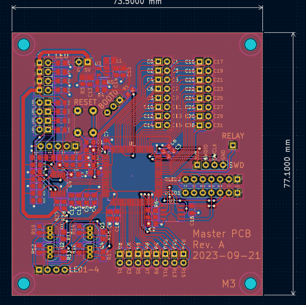
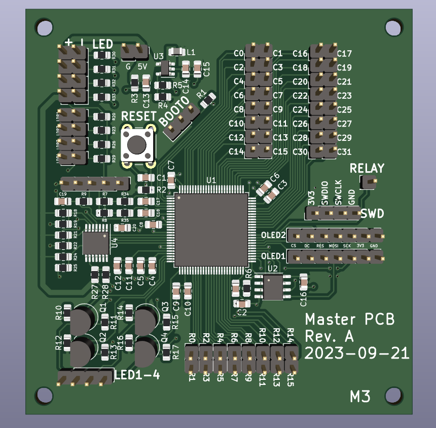
Although we haven’t found any issues with our master PCB, we decided to make some revisions for convenience for future testing. This mainly consisted of expanding the PCB size to 100x100mm and placing components more conservatively, giving us much more room on the board. The only additional components include ESD protection ICs on some of the external signals, and an optional external oscillator.
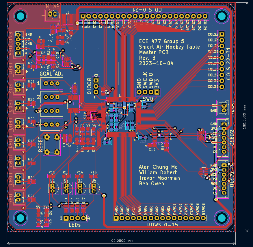
Figure 1: Master PCB Rev. B layout
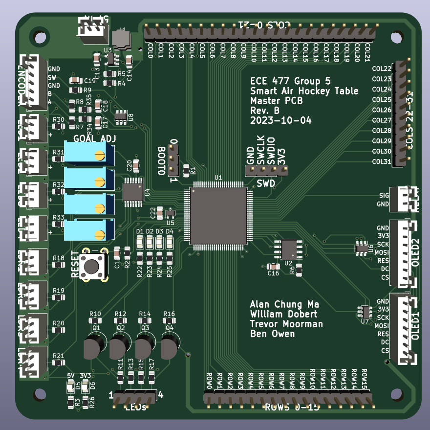
Figure 2: Master PCB Rev. B render
Master PCB soldering
Our Rev. A board still needed components placed. I spent a lot of time putting everything on the board, and we were able to test connecting and flashing to the STM32 before the team left for break. A picture of the PCB can be seen in Figure 3 and an image of us connected to the STM is shown in Figure 4.
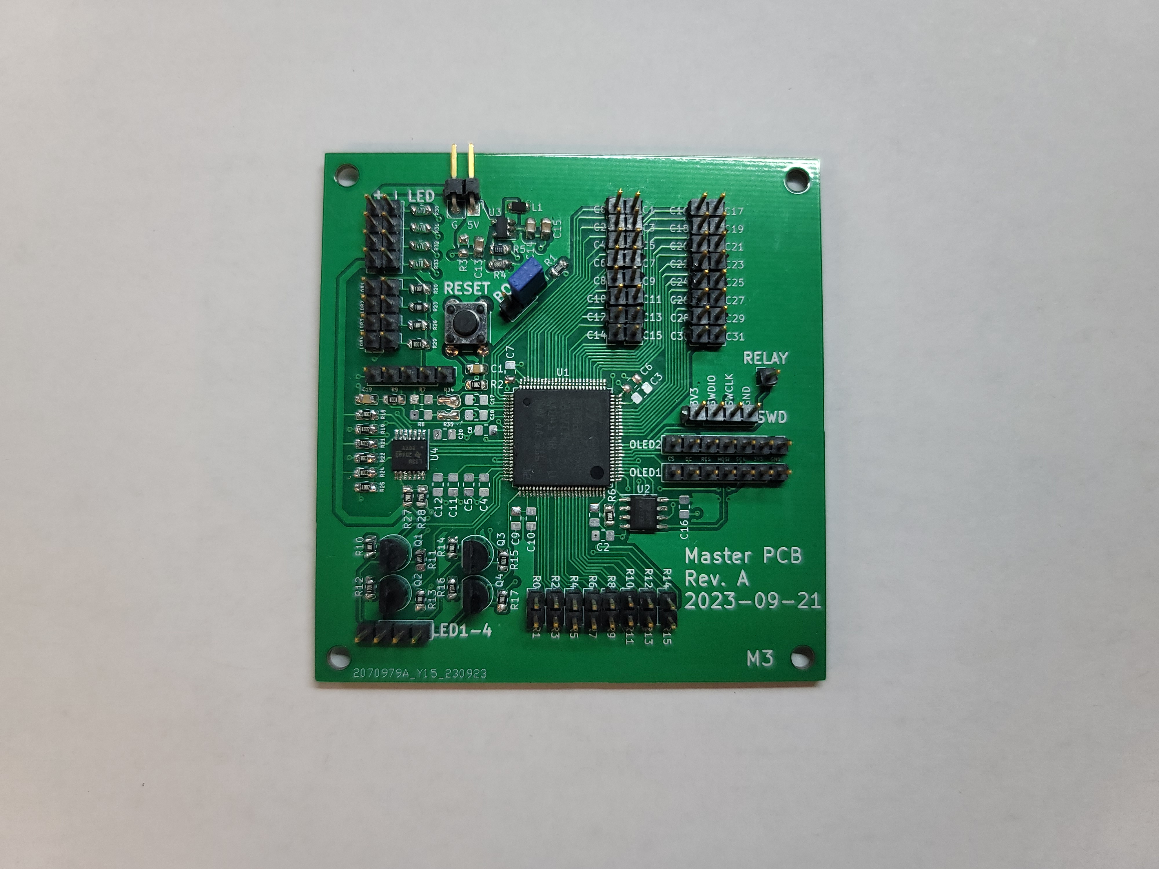
Figure 3: Master PCB Rev. A
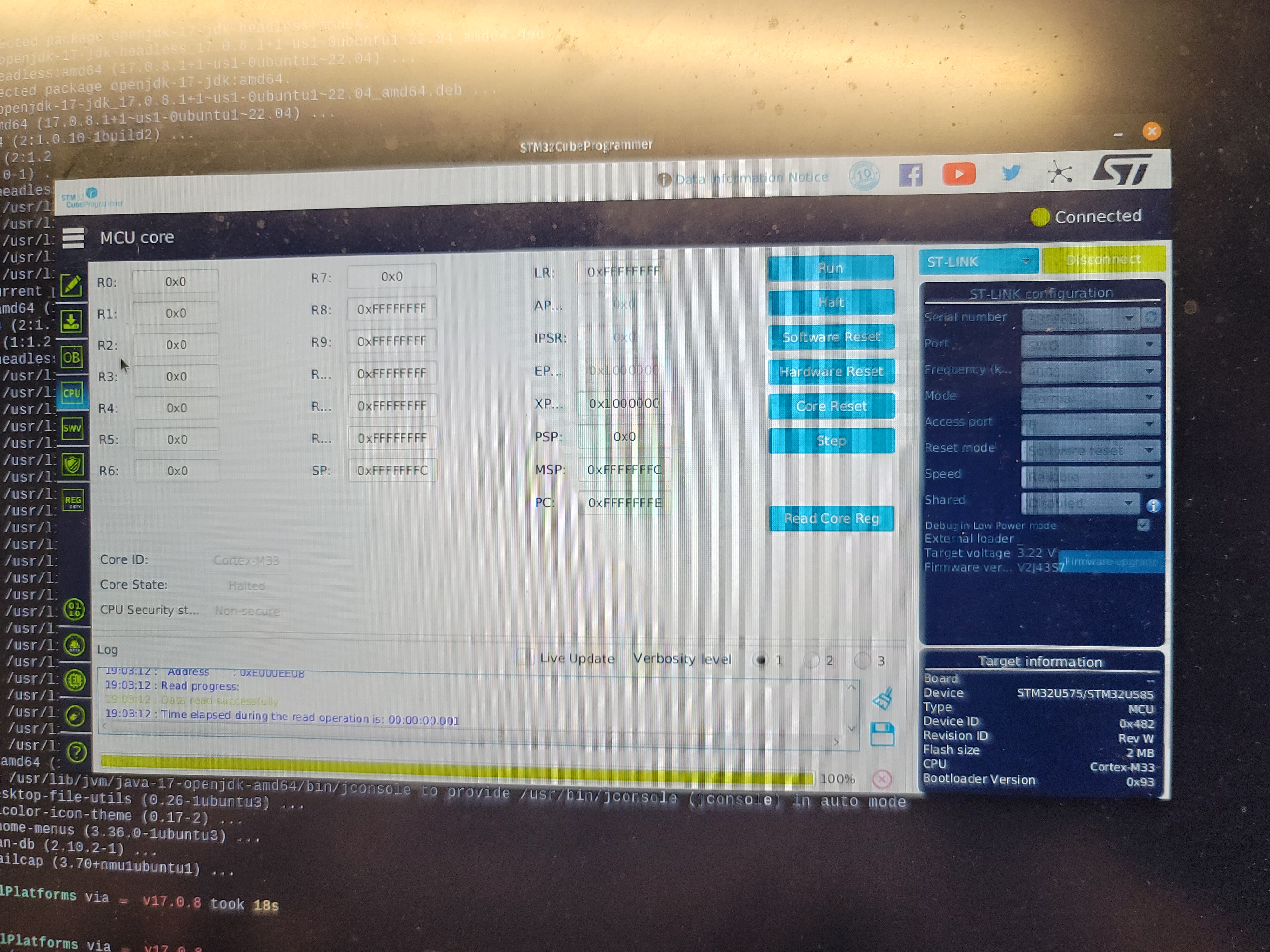
Figure 4: Connected to STM32
Sensor PCB soldering/testing
We put together 8 of our sensor PCBs, and tested the interconnection feature of the boards. We were able to send LED data across multiple boards. We were also able to see hall effect sensor data, also across multiple PCBs. An image of the connected boards can be seen in Figure 5.
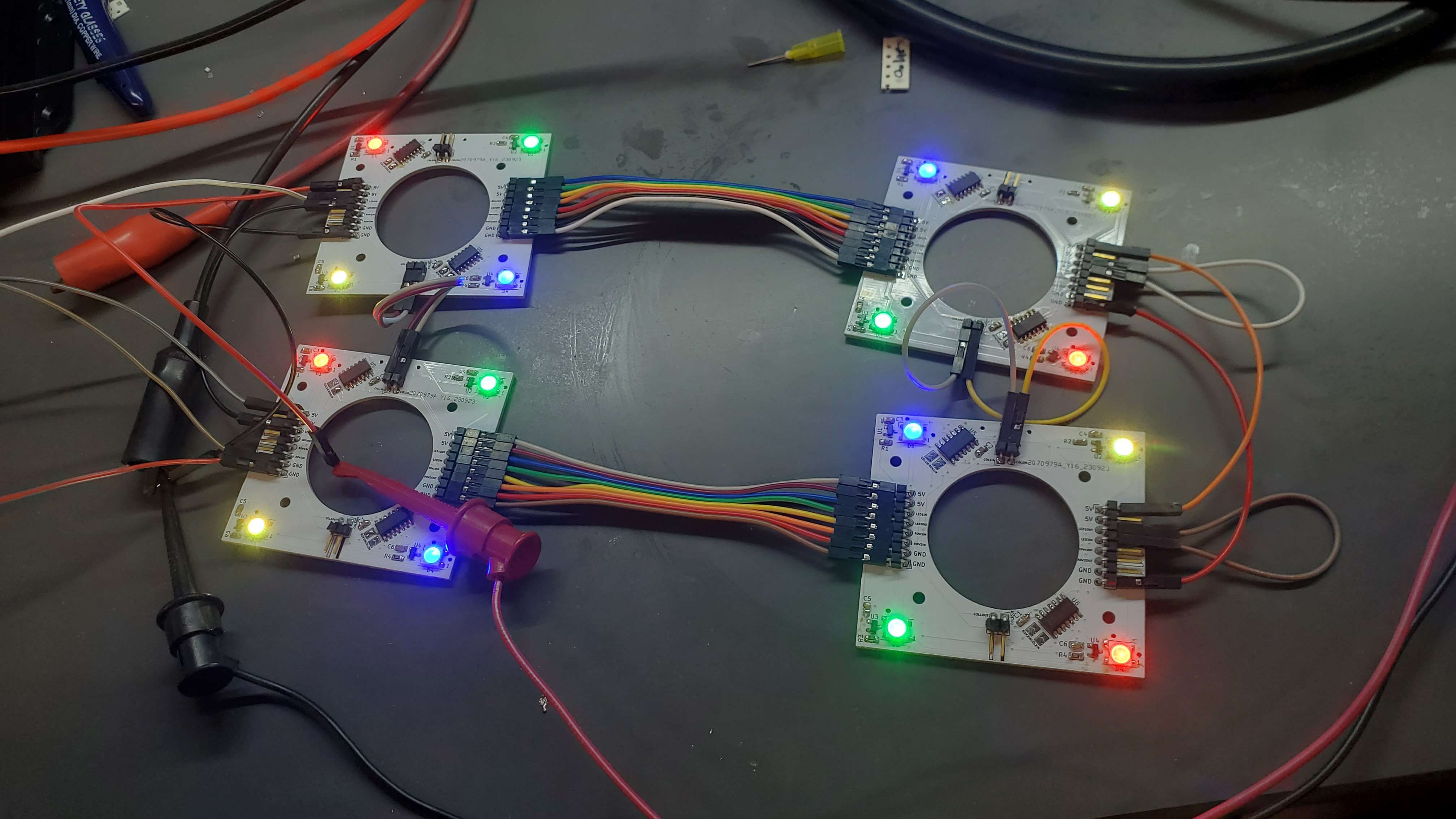
Figure 5: Sensor PCBs
Next steps
Midterm design review presentation
Top of the priority list is finishing and practicing our design presentation. We have multiple PCBs, revisions, and schematics, so there is a lot to cover.
Sensor PCB soldering
We want to test a full row of sensor boards (16 boards) before ordering the rest. This is going to involve some time to solder all components and test everything.
Master PCB testing
We need to verify all of the components combined on our master PCB. This involves slow testing of each component. Some of these can be ported from our Nucleo testing, but will still be time consuming.
Week 6
Date: 2023-09-29
Project Hours Since Last Report: 10
Total Hours: 74
Description of Project Design Efforts
This was exam week, but luckily we were in a position to order components, mainly our PCBs.
PCB Review
Buck converter
Before ordering PCBs last week, we made some final changes. The biggest change involved the buck converter. We ended up using copper pours to more closely match the datasheet. A screenshot showing our newer copper pour layout can be seen in Figure 1.
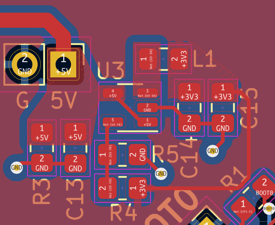
Figure 1: Buck converter PCB layout
5V power trace
We also added a thicker 5V power trace to power our LEDs, LDRs, comparators, and other miscellaneous 5V components on the board. We already had a 3V3 and GND pour, but the 5V line was a thin trace spanning multiple components. To give ourselves more room for higher current draw, we expanded our board and added a thick 1mm trace to carry the 5V power line to many components. This new power trace can be seen in Figure 2.
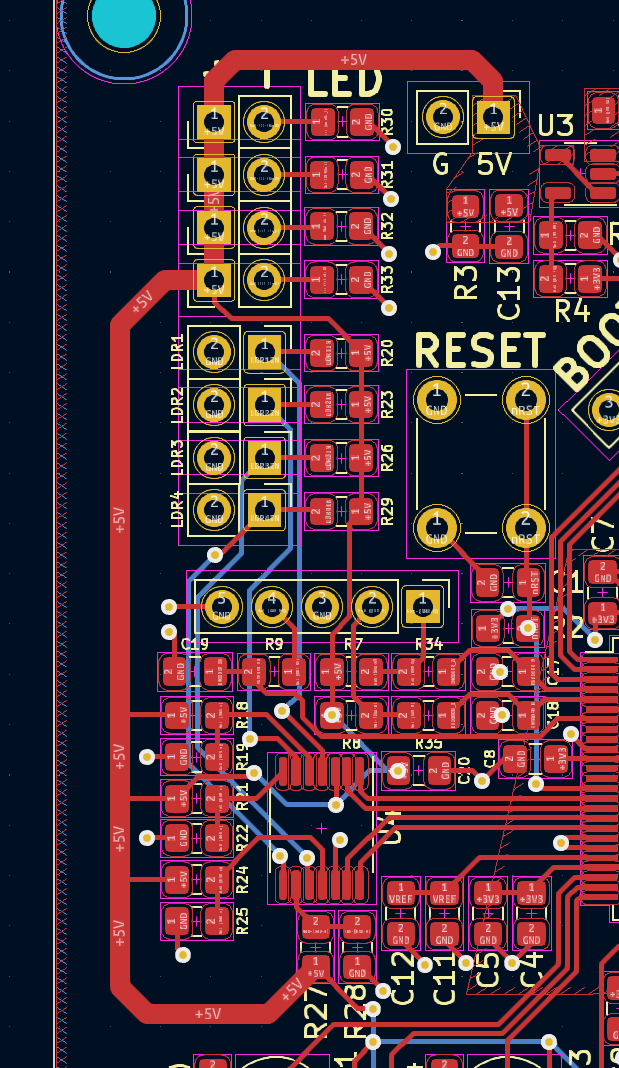
Figure 2: 5V power trace
Some images of our PCBs can be seen in Figures 3 and 4.
 |  |
|---|---|
| Figure 3: Master PCB | Figure 4: Sensor PCB |
Testing of new components
Many components came in, including our air blower, OLED displays, connectors, power supply, and outlet relay. Although there wasn’t much time to test due to our team’s exam schedule, we were able to test our power supply and outlet relay. To do this, we cut a PC power cable and connected the hot, neutral, and ground wires to the correct screw terminals on our power supply. We then connected this power supply to the outlet relay, which can be controlled with a low-voltage DC signal. We connected this to our power supply, and tested the functionality with both 3V3 and 5V. A video showing this testing can be seen in Figure 5.
Figure 5: Outlet relay testing and proof of operation
Next steps
PCB revisions
Getting closer to fall break, we want to make PCB changes to improve our design. Our first revision was to be in a position where we could prototype, but we already have a list of changes we want to make:
- Better placement of decoupling capacitors (under chip)
- Expand PCB size (100 x 100 mm)
- Larger mounting holes
- Better pin header placement (along edge of board)
- ESD protection for some GPIO
- Reverse polarity protection (if possible)
- Slight GPIO remapping to allow for easier rotary encoder implementation
OLED driver
I am going to help test the new OLED displays and create a driver for easier usage. I am planning to define an alphabet for character displays, since this display is designed to display graphics, not just text. This means that we will have to define each letters’ pixel arrangement.
Week 5
Date: 2023-09-22
Project Hours Since Last Report: 25
Total Hours: 64
Description of Project Design Efforts
Schematic/PCB design
All of my efforts this week went into creating/finalizing the schematics for our master PCB and sensor PCB designs with Trevor.
Master PCB
The primary schematic contains all external connectors and signals that are going off-board. We used KiCad’s hierarchical schematic function to keep everything clean. You can see the main STM32 block in the center, connected to our EEPROM, OLED connectors, LEDs, LDR inputs, and row/column hall effect sensors.
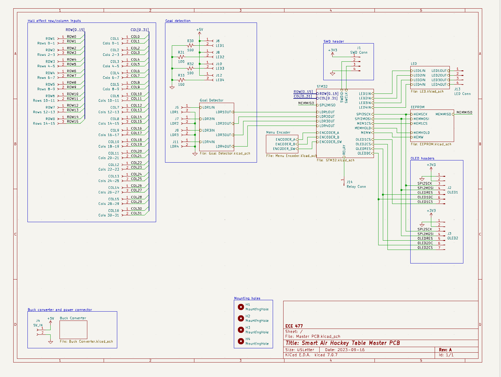
Figure 1: Top level schematic
The STM32U585 is the microcontroller we decided on, and the schematic with the STM32 on it simply defines all of the pin connections, reset button, decoupling capacitors, and BOOT0 jumper. We verified the pins’ position and function using the STM32CubeIDE IOC program to make sure we were using correct pins (peripheral assignment, 5V tolerance, etc.)
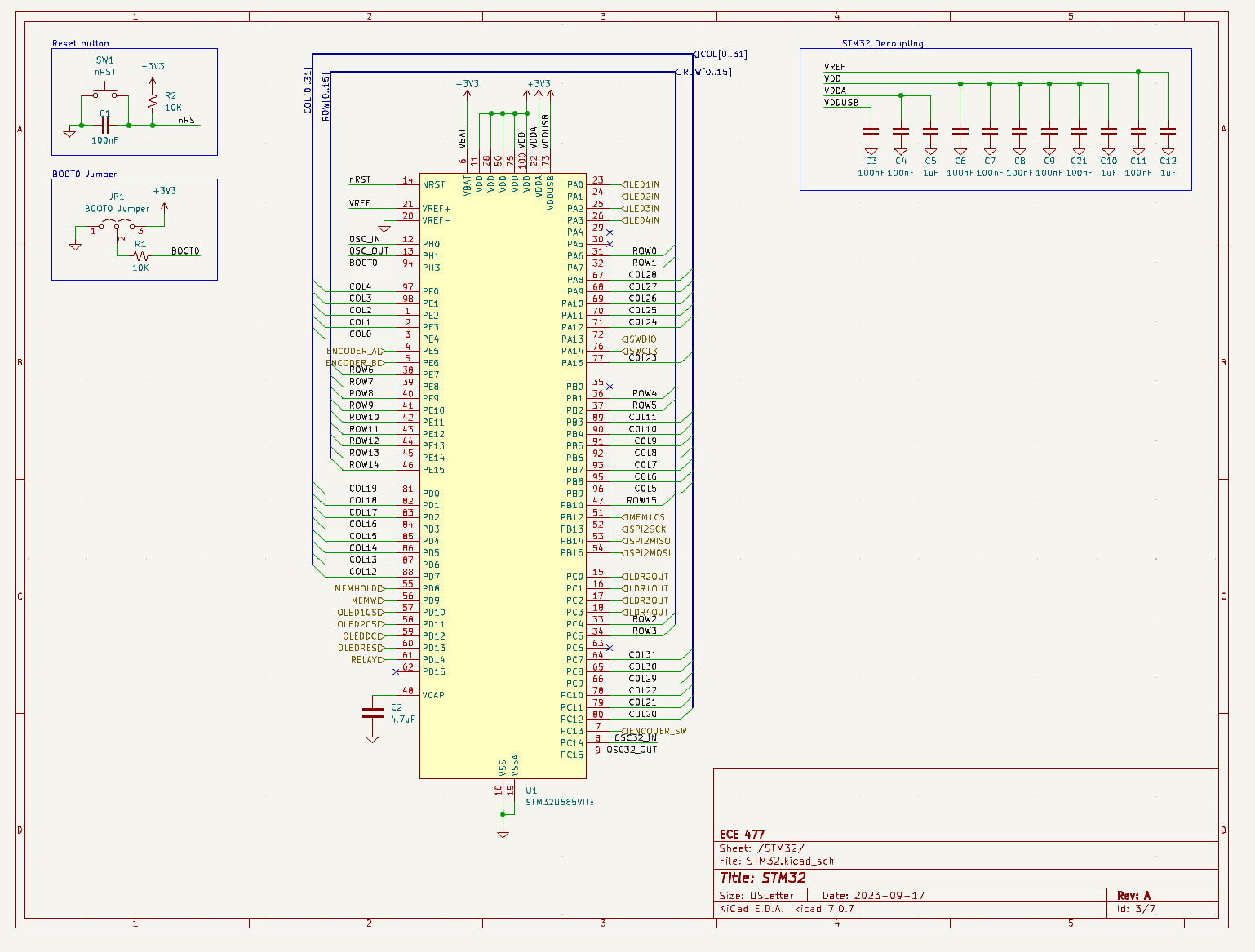
Figure 2: STM32 schematic
To satisfy one of our PSDRs, we are implementing a buck converter to power our STM32. We chose the TLV62568 due to its simplicity, small size, low price, and high enough output current at 1 amp. The schematic for this regulator can be seen in Figure 3.
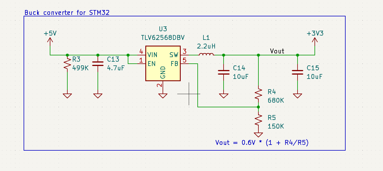
Figure 3: Buck converter schematic
Goal detection is achieved by using an LED/LDR pair. This analog value is then compared against a reference voltage (created with a voltage divider) in a comparator circuit to convert this analog value to a digital value. This digital signal is then connected to the STM32 to determine if a goal has been scored. The schematic for our goal detection comparator circuit can be seen in Figure 4.
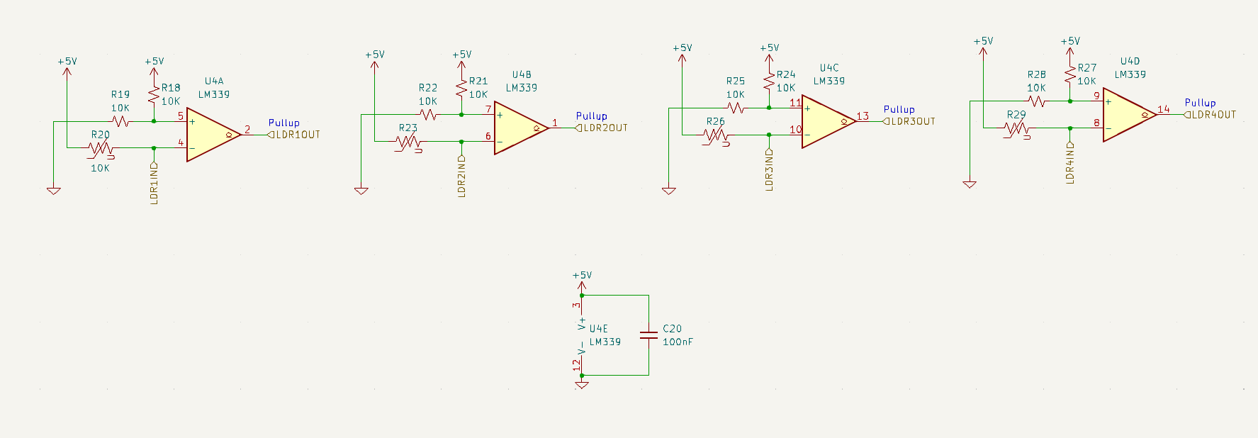
Figure 4: Goal detection schematic
One of our stretch goals is to have a menu system displayed on an OLED to allow users to change brightness, goals required to win, and other settings. To allow the user to interact with the microcontroller, we are attempting to implement a rotary encoder with an integrated button. The schematic representing this circuit can be seen in Figure 5.
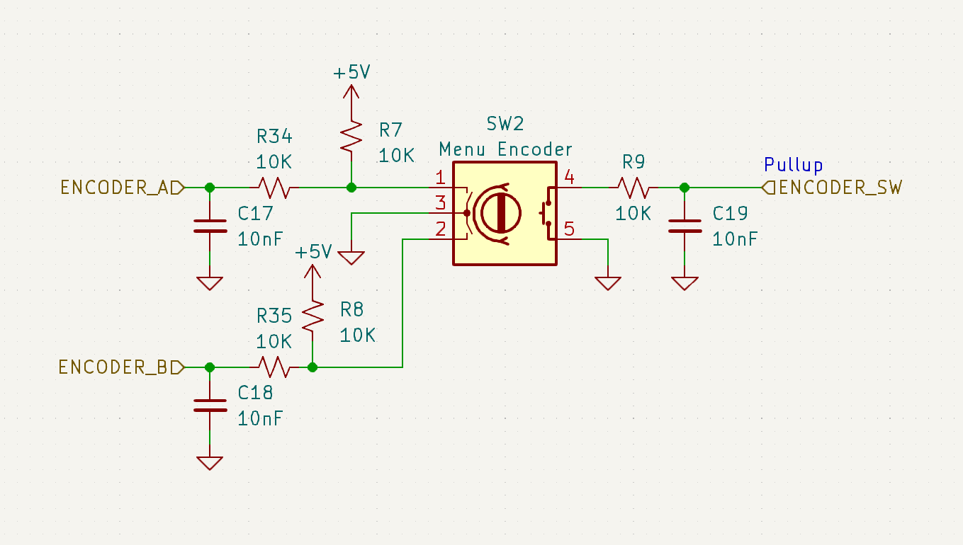
Figure 5: Encoder schematic
The LEDs are interfaced from the STM32 through level shifters. The WS2812B LEDs we are using run at 5V logic, and our STM32 can only provide 3.3V. We implement the level shifter that Will had been testing with to support up to four independent channels for the LED control. The schematic for these level shifters can be seen in Figure 6.
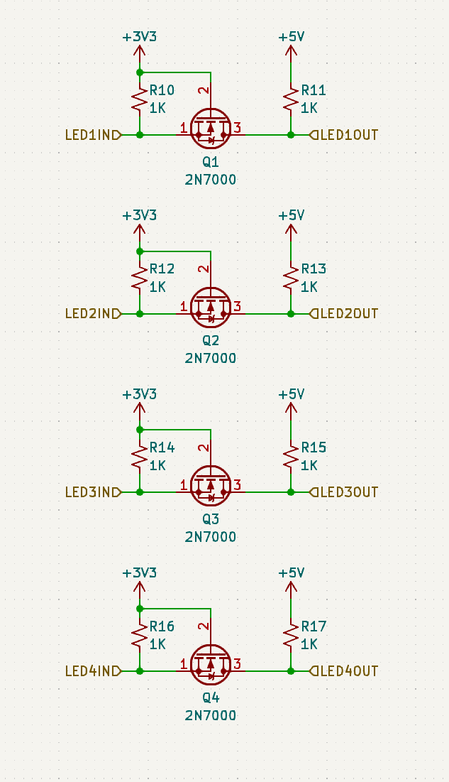
Figure 6: LED level shifter schematic
One of our other stretch goals is using an EEPROM to store table configuration and animation frames. This is interfaced with our microcontroller over SPI. The schematic representing this chip and its supporting hardware can be seen in Figure 7.
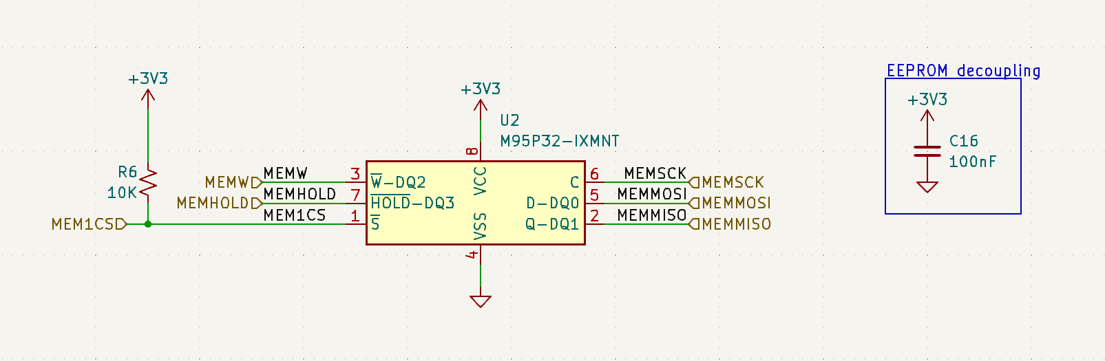
Figure 7: EEPROM schematic
After the schematic was put together, we routed the first revision of our PCB. We want to get these ordered as soon as possible to allow for debugging and ordering of a second round before week 8. Many considerations, such as power requirements, decoupling capacitors, and communication protocols were considered when laying out components. A side-by-side view of the layout and 3D renders can be seen in Figures 9 and 10.
 |  |
|---|---|
| Figure 9: Master PCB layout | Figure 10: Master PCB 3D render |
Sensor PCB
In addition to the master PCB, I worked a lot with Trevor doing the same process for our hall effect sensor PCB. This was a simpler design. We have 4 hall effect sensors per PCB, using AND logic gates to convert these values to rows/columns. The data can be daisy-chained between PCBs, allowing the microcontroller to only need 48 GPIO inputs to determine the position of the puck. In addition to the sensors, the schematic contains the LEDs and LED data signals, power passthrough for components on the boards, and solder jumpers to ensure non-floating inputs on our logic gates for PCBs with only two inputs (the first PCB in each row/column only has 2 inputs since there is no data being passed into it from another board). The current schematic for this design can be seen in Figure 11.
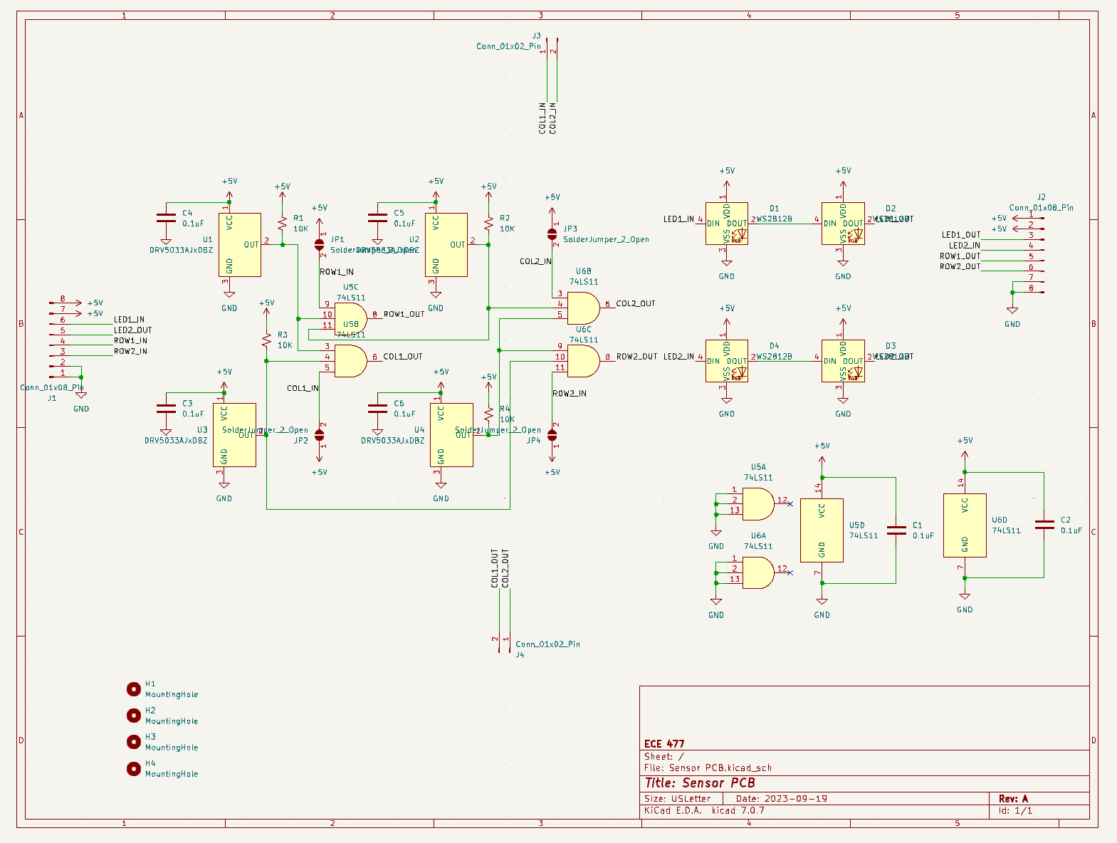
Figure 11: Sensor PCB schematic
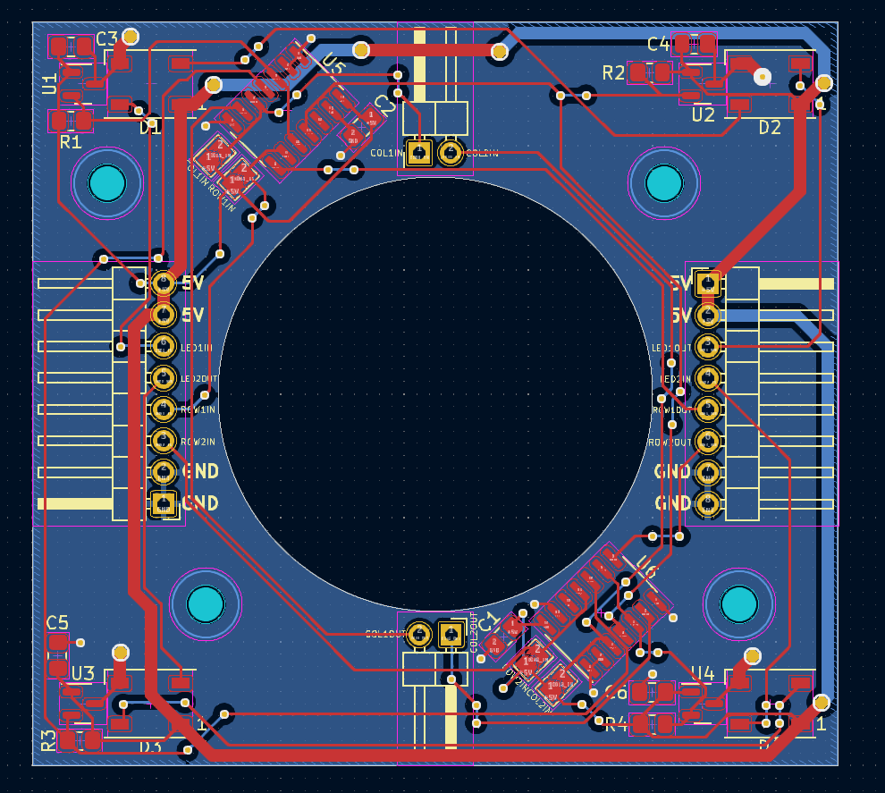
Figures 12 and 13 show the routing and 3D render for this PCB. The main considerations were the edge connectors allowing for PCB-to-PCB connections, as well as a fixed 50mm distance between the hall effect sensors. The large hole in the center is to assist in airflow for the PCBs mounted directly over the blower on the table.
 |  |
|---|---|
| Figure 12: Sensor PCB layout | Figure 13: Sensor PCB 3D render |
Next steps
PCB review/ordering
I will probably look over these boards for a bit longer to try and find any mistakes in the schematic/routing before we order the boards. Hopefully everything looks good, but I expect to spend a few hours checking again.
Table state machine
Once the PCBs are ordered, we will need to wait to do anything hardware related until they arrive. I will be helping the other team members, primarily on the firmware for the game state machine. The current tasks include:
- Creating the game superloop triggered off of a timer
- Defining all of the states for the game
- Defining all of the criteria to change states
- Determining where/when to use interrupts and when to use polling from the superloop
Week 4
Date: 2023-09-15
Project Hours Since Last Report: 12
Total Hours: 39
Description of Project Design Efforts
Puck tracking/hall effect sensors
The new magnets arrived and we found them to be much higher quality (and much stronger) than the ones we were using previously. However, with our new design for battleship-style puck position tracking, we no longer need to use analog hall effect sensors, and can instead use simpler digital hall effect sensors. Unfortunately, however, the ECE shop doesn’t stock these models of sensors, so we will be ordering some this week along with our first round of PCBs.
Individually-addressable LED driver
The majority of my time was spent working with Will on a driver to control the individually-addressable LEDs we will be placing under the table. This is because we are not using a library from another source, but wanted to take advantage of the peripherals on our STM32 to maximize performance. The driver we came up with uses a timer in PWM mode with the DMA to adjust the pulse width in order to create an 800KHz signal for the LEDs.
My work on the driver included the initial setup of the timer at the correct baud rate. After trying to adjust the PWM duration using the CPU, we found that we were unable to change the timer’s CCR register fast enough for reliable data transmission. Therefore, we pivoted to a DMA-based design, where we store the CCR register values in memory and allow the DMA to cycle through them automatically. This DMA event is triggered by the timer interrupt, so there is virtually no CPU overhead and no processing needs to occur to display the frame data on the LEDs. We were able to achieve refresh rates well above 60Hz, likely into the hundreds (too fast to see with the naked eye). This will obviously lessen with more LEDs in the chain, but it is very promising for our table’s design.
An example of the work I put into the driver can be seen in Figures 1 and 2.
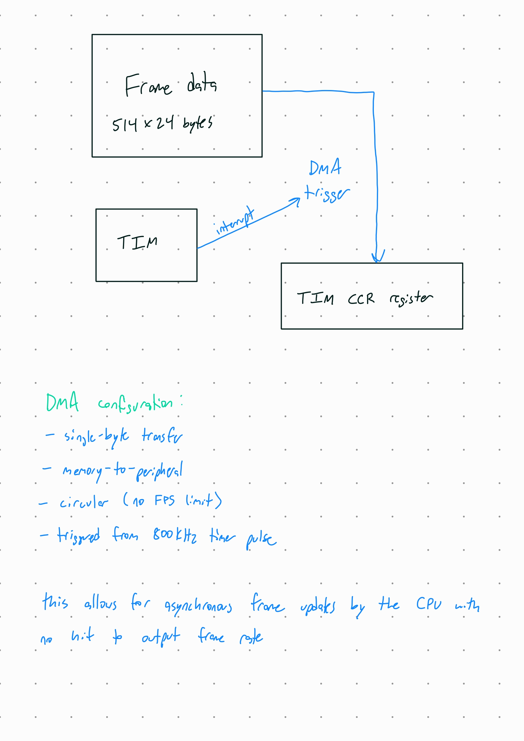
Figure 1: LED driver with DMA brainstorming
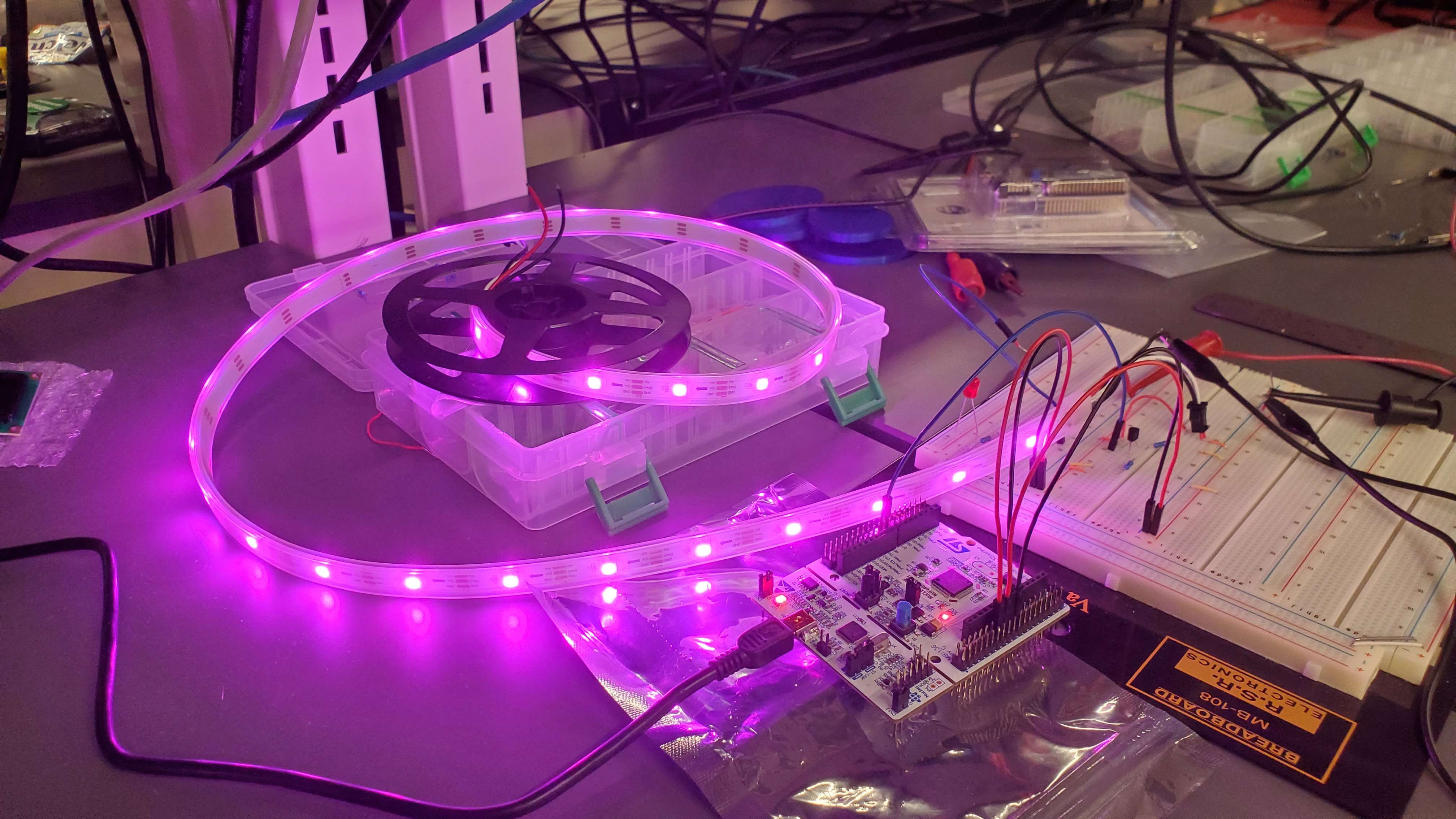
Figure 2: LED driver demonstration (cycles between RGB spectrum)
Microcontroller research and part selection
Our team met for around 3-4 hours on Thursday to try to finalize which microcontroller we wanted to order and implement for our first round of PCBs. After a long discussion, we decided on the STM32U585 series, which falls in their “ultra-low power” family of microcontrollers. Although power isn’t the biggest concern on this project, this particular microcontroller offers a relatively fast clock speed of 160MHz, as well as a large ROM size of 2MB.
This microcontroller comes in a LQFP100 package, which will be relatively easy to solder and has just enough I/O for our application. We determined in our meeting that we need 68 I/O pins, and this microcontroller offers 82. We also consider other families of STM32, such as the F7 and H5 series, but we found that they were either too expensive, too large, or otherwise unnecessary for the scale of our project. The U5 family is a good balance of the performance characteristics we need for our project.
Microcontroller pin determination
After deciding on a microcontroller, I spent some time creating a document where we can start to assign pins on the microcontroller to peripherals in our project. This is going to be a time-consuming process, and this is after the hours we already spend transposing the information from the datasheet to a spreadsheet for our own use. So far, I spent time going through each pins’ alternate functions and additional functionality and marked anything of interest, such as timer channels, SPI channels, oscillator inputs/outputs, etc. I also marked pins that we will leave open, such as the BOOT0 pins to force bootloader booting, the SWD debugging pins, and the reset button pin. An image from this document can be seen in Figure 3.
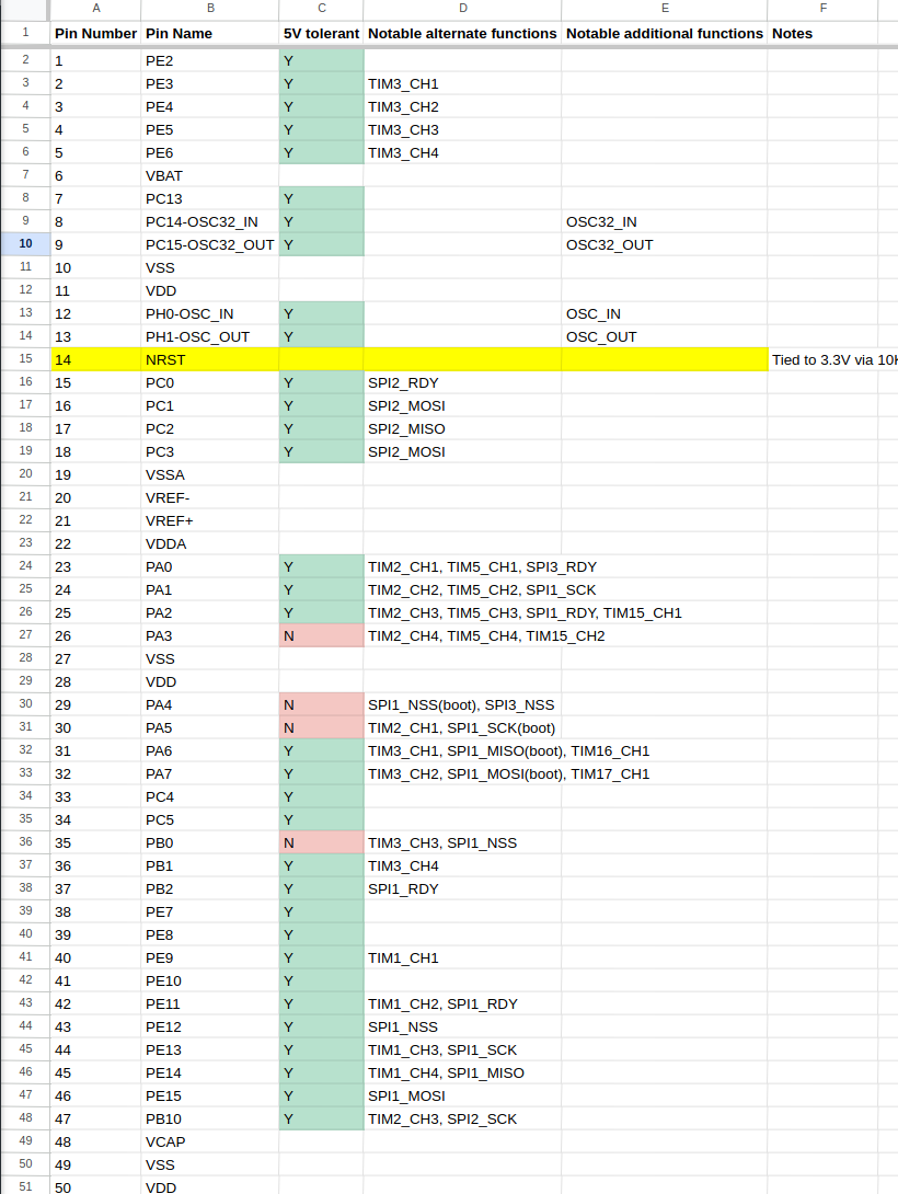
Figure 3: Some of the microcontroller pin descriptions
Next steps
PCB Design
PCB design is the primary thing I will be working on this week, as we want to get these in hand as soon as possible. Furthermore, we aren’t able to test our final components since they are all SMD, so we need a board to mount them to for further testing.
- Trevor and I will continue determining pin selections for our microcontroller and laying this design out on our first round of PCBs
- Current master PCB parts to be implemented:
- STM32U585 footprint with SWD programming header
- Buck converter to power STM32 from a 5VDC source
- Connections to OLED displays, hall effect sensors, and LEDs
- Current sensor PCB parts to be implemented:
- SMD hall effect sensor (likely TI TMAG series) footprints in 2x2 grid per PCB
- LED footprints next to hall effect sensors, also in a 2x2 grid
- Footprints for digital logic gates to convert to row/column position data for the microcontroller
- Connection to the master/other sensor PCBs to daisy chain the signals along the boards
Week 3
Date: 2023-09-08
Project Hours Since Last Report: 15
Total Hours: 27
Description of Project Design Efforts
Puck tracking
I spent a lot of my time brainstorming with Trevor various ways to enhance our multiplexing of the 512 estimated hall effect sensors we will be implementing. Our first solution involved having a dedicated STM32 on each “row” of PCBs to interface with only the hall effect sensors in its row. These microcontrollers would then report back to the master microcontroller the status of its hall sensors, where this data would be aggregated and any game-state related steps could be taken. However, this solution involves over 16 total microcontrollers, which is complex and expensive.
We then thought of using an op-amp/comparator circuit to convert the analog values to digital on each PCB, and then simply multiplex the hall sensors using analog electronics. This would be simpler to implement, but the amount of routing would make this infeasible. Either each row would have to be connected differently, or all 512 signals would have to converge at a single PCB, making routing virtually impossible. However, during the brainstorming for this idea, we came up with our likely path forward.
After drawing out a grid of hall effect sensors, we realized that by simply ORing together each row and column of sensors, we could obtain the given row and columns of active hall sensors, allowing us to pinpoint the puck’s location with little overhead. In terms of I/O, we only needed (total number of rows) + (total number of columns) GPIO pins; in our current design, this number totals to 48 pins. Furthermore, there are no communication protocols adding delay, and the PCB routing becomes identical for every single PCB (excluding the master) with no additional microcontrollers. I plan to flesh this idea out on a breadboard this weekend/into next week to prove feasibility.
An example of this design can be seen in Figure 1:
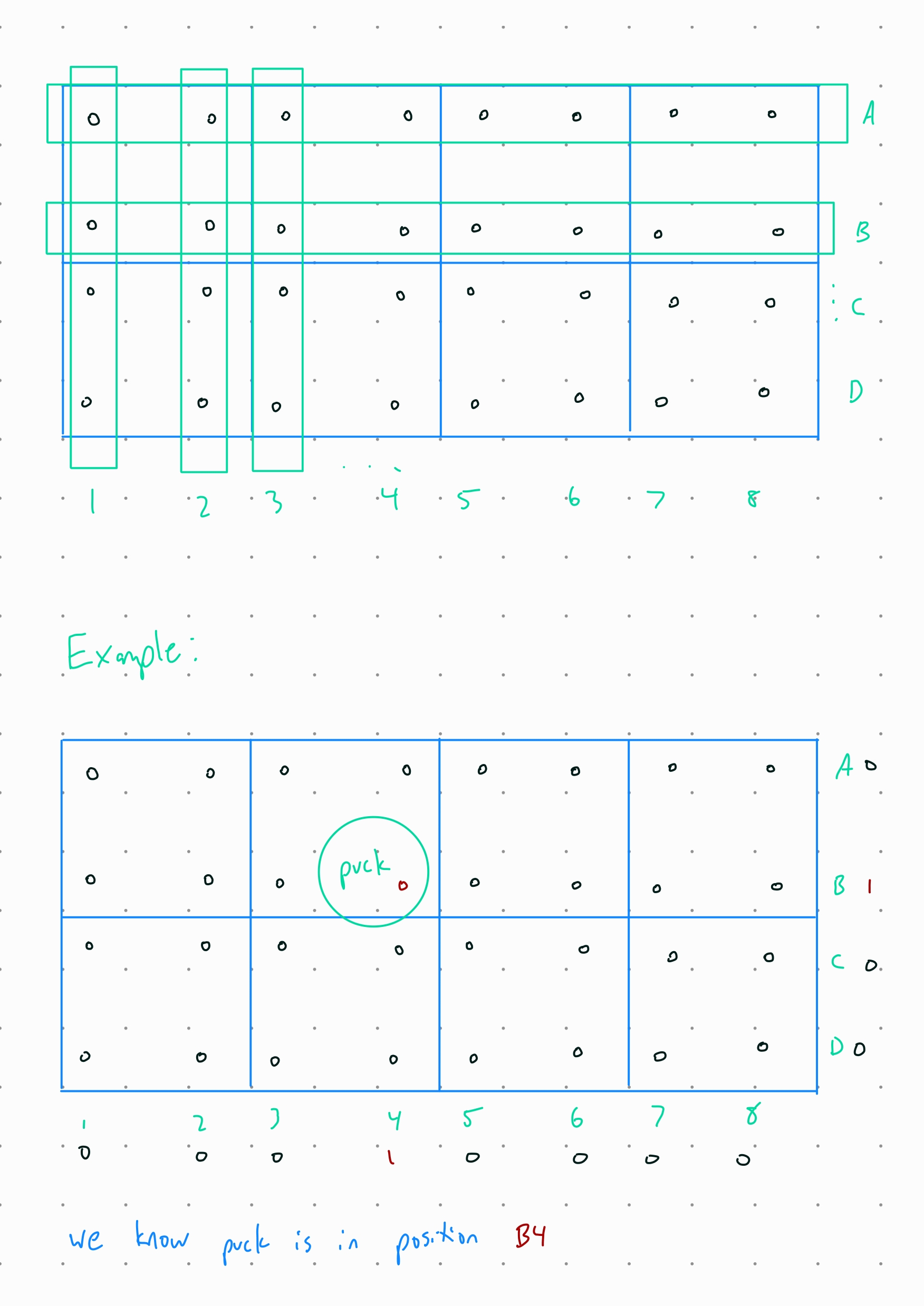
Figure 1: “Battleship” hall effect position demonstration
Magnet research and part selection
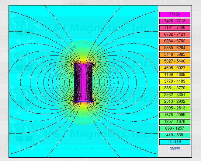
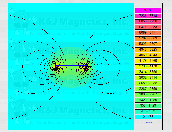
The other topic Trevor and I met about was determining which magnets we wanted to procure to continue testing. We did a lot of background research and learn about different magnet grades. It appears that the current “top grade” of consumer magnets is N52, where the N stands for neodymium and the 52 refers to a complex equation relating to its field strength. Common magnets are typically N35 or possibly N42, so obtaining higher-grade magnets should improve our magnetic field.
The magnet supplier we ordered magnets from, K&J Magnetics, Inc., lists many technical resources with many of their magnets. We originally were leaning towards purchasing small cylinder magnets such as this D12-N52 model, as the surface field was listed as 7179 Gauss, higher than many larger disc magnets. However, this comes at the expense of pull force, which at the time, we didn’t believe was as important as field strength. After looking at disc magnets, such as this DX02-N52, we noticed that although the surface field was lower, it was more concentrated around the edges, and was in fact much stronger than the cylinder magnets.
We continued to do research, and eventually found this page discussing how the surface fields are measured. Reading this revealed that the magnets are measured at the center along the axis of the magnetic field. Since the field is concentrated near the edges of the disc, this leads to much higher readings for cylinders, even if they are actually weaker in practice than discs. This led us to choose the disc magnets to continue our testing in future weeks.
Figures 2 and 3 contain a comparison of the cylinder and disc magnetic fields:
 |  |
|---|---|
| Figure 2: Magnetic field drawings for a cylinder magnet provided by K&J Magnetics, Inc. | Figure 3: Magnetic field drawings for a disc magnet provided by K&J Magnetics, Inc. |
LDR goal detection
My primary goal was to determine a reliable way to detect a goal from the air hockey puck. I originally was testing IR circuits, using an IR LED and IR photodiode, but found detection complicated and unreliable. After some thought, I decided to try a simpler LED + LDR combination, using analog circuity to convert these readings to a “digital” on/off signal.
I eventually made a comparator circuit using a reference voltage (created with a voltage divider), and a second voltage divider combining the LDR and a variable resistor (in my case, half of a potentiometer). This combination was hooked up to an indicator LED to easily observe the output. After some tuning, this method was shown to be very reliable and easy to adjust the threshold of on/off if needed. These factors led to this design becoming the primary way we will pursue goal detection. Additionally, because of the circuit’s low cost, we can implement 2 on each goal to add reliability in the event that one of the LDRs doesn’t trigger or something breaks over the life of the table.
A picture of the breadboard containing this circuit can be seen in Figure 3:
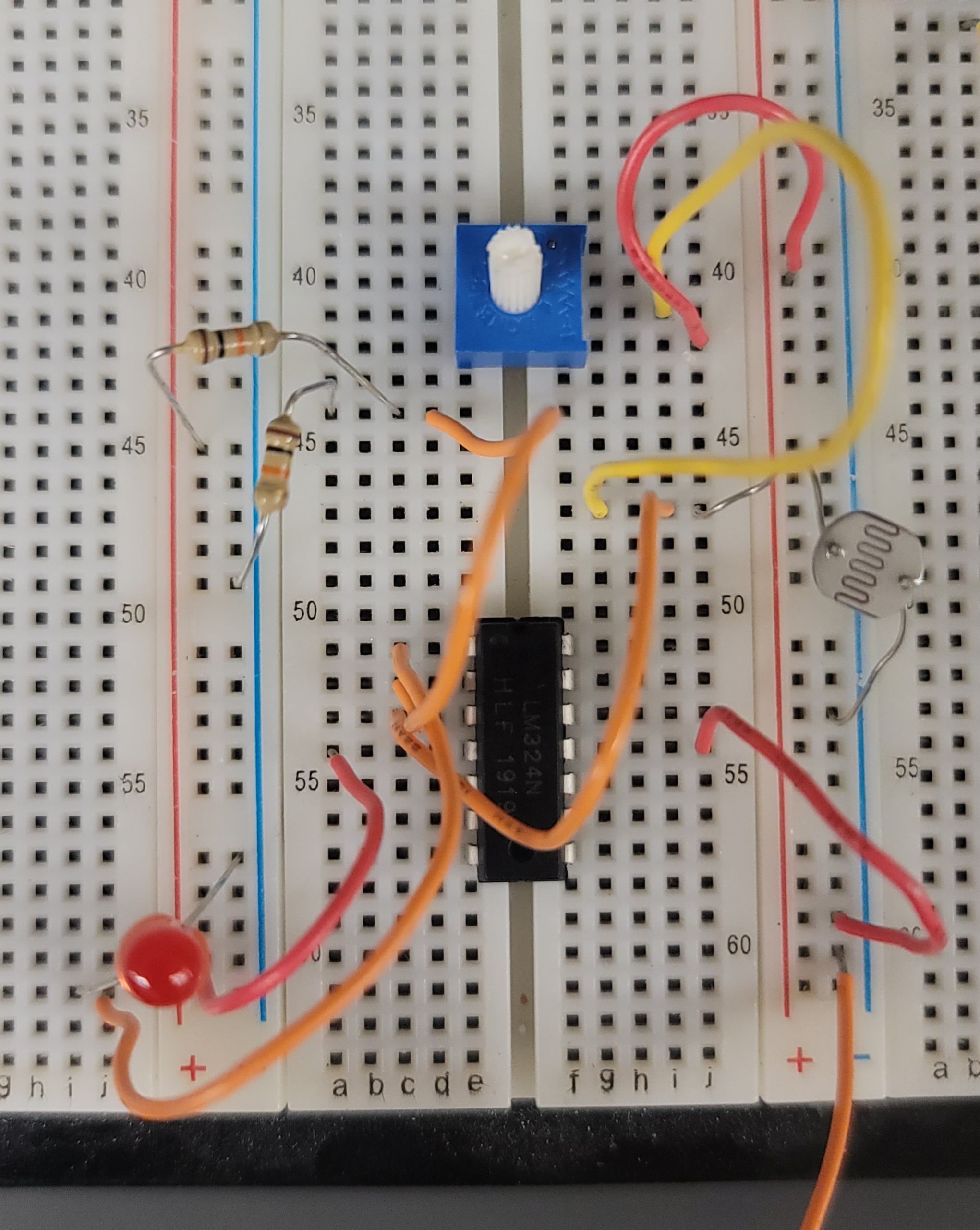
Figure 4: Image of breadboard LDR goal detection circuit
A schematic representation of the circuit can be seen in Figure 4:
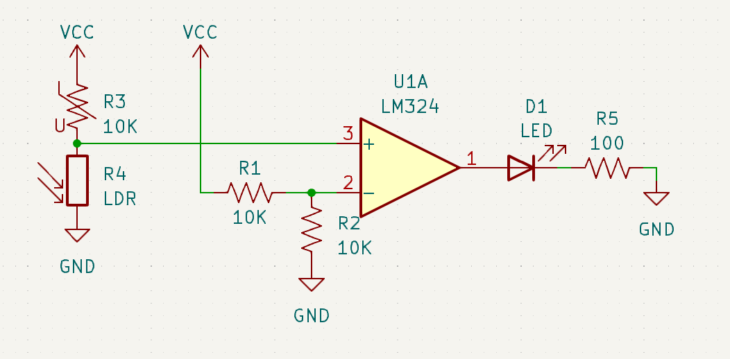
Figure 5: “Battleship” hall effect position demonstration
Next steps
Puck tracking
- I will build a 2x2 (or larger) hall effect grid on a breadboard and connect using the digital logic mentioned earlier
- Trevor and I will test the new magnets when they arrive to try to determine the desired air gap for our table
- Once this is completed, we will likely need to construct a miniature version of the table to continue testing the hall sensor system
Magnet research and part selection
- If testing goes well with the parts that are on order, nothing more needs to be done
- Current testing includes center magnet positioning and a ring of magnets on the puck closer to the edge
- If testing does not go well, we may reconsider the magnet layout on the puck and/or the magnet type
LDR goal detection
- I will work with Trevor and his comparator-focused design to finalize this circuit, including redundancy and potentially testing the digital interrupt with our STM32
LED interfacing
- Most of my time will likely be spent here; I will be helping Will with LED communication
- He currently has implemented a basic timer serial interface, but we will need to implement DMA for optimization at higher refresh rates
PCB design
- I will be working with Trevor to put together the first round of PCBs to order
- PCBs will contain:
- LED footprints and wiring
- Hall effect sensor footprints and wiring
- Analog/digital logic IC footprints and wiring
- Connectors/pads to connect PCBs to each other for larger testing
- (Potentially) an STM32 footprint to test with embedded STM32 soldering and programming without a Nucleo development board
Project description and PSDRs
- As I get more testing and feedback from other group members, I will be helping revise these to get them finalized as soon as possible and update the website
Week 1 & 2
Date: 2023-09-01
Total Hours: 12
Description of Project Design Efforts
I spent most of these two weeks doing background research and helping complete team tasks relating to the project. Most of my expertise relates to my past embedded experience, so I have been using most of this time to brainstorm potential solutions to the numerous engineering challenges and helping define constraints for our finished project.
Background research
Most of the background research I did over these first two weeks related to feasibility analysis for various components. Due to the scale and complexity of our table, I investigated different possible solutions for puck tracking, communication, and LED manipulation. I analyzed prices and datasheets for various sensors, checked what parts we could potentially obtain for free using the ECE shop catalog, and brainstormed a few solutions for high speed communication of dozens of microcontrollers. Heading into the next few weeks, this research will be tested for real-world feasibility.
STM/STM communication
My primary research was trying to find which STM32 models would support our worst-case situation: one STM32 for each daughterboard PCB. Our master STM32 would need to be high speed and have lots of communication peripherals and I/O pins. After lots of evaluation, I found the STM32F446RE, which is both in stock and cheap. It can run at high speeds of up to 180MHz, but more importantly, has lots of onboard protocols, including quad SPI and up to 114 I/O, though we will have less available to avoid the BGA packaged version.
Another microcontroller we may explore is one of the lines with OCTOSPI. This would allow us to communicate with all of the rows at the same time. However, for potential expandability of our table, this doesn’t solve the overarching problem.
Team Meetings
Our team held a few meetings to work on the team assignments. These meetings were mostly used to outline each member’s responsibility and split the work according to our strengths, but we also brainstormed ideas for our tables. Much of the time spent in these meetings is described in the other two sections for this week’s progress report.
Team Assignments
The first two weeks had both the revised initial project proposal, final project proposal, and the function specifications due. I spent a lot of time revising our initial proposal, primarily researching and decsribing a more relevant existing product to include in our market research section of the document. For the final project proposal, I primarily helped with the initial budget estimation, using hypothetical parts and current market pricing to create a rough price estimate for our project.
Brainstorming PDF
Notes from my brainstorming and diagrams about my communication brainstorming can be found at this link: Brainstorming PDF.